This is really part 2 of Emulating a hardware ROM in real time with an STM32F4. In that post I used a cheap STM32F407 board to emulate some ROMs and some IO ports for an Acorn Electron. ie. The Electron thinks it has a bunch of hardware attached, but it’s simply the STM32F407 board pretending to be these things;
- A few sideways ROMs
- Some IO ports that have an SD card attached to them.
It worked by effectively polling for changes in the main phi0 clock of the 6502A in the Electron.
The goal was to be able to use MMFS, which gives you access to virtual floppy disks.
And it all worked … for me.
I only recently posted to the stardot forums about my project, and for whatever reasons I reminded myself that it would be much nicer if the code used interrupts. In the original post I think I tried to get interrupts working and failed, and opted for using continuous polling of the phi0 signal. The huge negative of using polling is that your code is locked in a polling loop and you can’t do much else. Polling was fine for the MMFS use case, as MMFS itself bitbangs the SD card to access it, and all I was doing was ‘passing through’ the right bits at the right time … so to speak. With interrupts you can do other stuff at the same time. I’d been able to get interrupts to work on an Amstrad CPC-464 with a Z80A CPU, and I always thought that the reason I couldn’t get interrupts working on the Electron , but could on the Amstrad was that the timing on the Amstrad was a bit ‘less tight’ compared to the Electron. But anyway, posting to the stardot forums inspired me.
So I had another go at getting interrupts to work on the Electron.
Initially I couldn’t get it to go again. After hacking away , and working out the technique of using the floating point registers as general purpose global data registers I eventually got it to work for me. So the key thing with using interrupts is that you don’t have much time to do stuff. Effectively the phi0 clock is connected to a GPIO pin (in my case PC0) of the stm32f407. All CPUs have some interrupt latency, the time between the physical interrupt event and the first line of your ISR (Interrupt Service Routine). You would think this is super fast with a modern CPU, but it’s often disappointing compared to the older CPUs. Modern CPUs often have more registers and generally ‘more stuff to do to save the state of the processor at the time the interrupt occurred’. Whereas a 6502 or a Z80 would generally just jump to a subroutine at the time of an interrupt and leave you responsible for saving most state, a modern ARM CPU will automatically save registers R0-R3 and R12 for you. That’s a lovely thing to do, but pushing those registers takes time, and then you have logically other effects such as cache misses/refills and so on.
Here’s a sample of the delay. In the logic analyser shot below, the top trace is the phi0 line from the 6502A, and the lower trace is the output of PA0. Effectively my code toggles PA0 at the start of the ISR. So the ISR is triggered on the negative edge of phi0 (even though most of the useful stuff happens after the positive edge. More on that later).
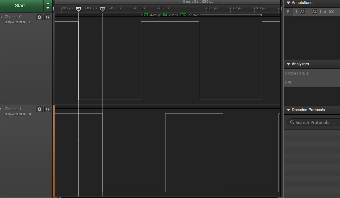
So according to that , my ISR has toggled PA0 low 100ns after the falling edge of phi0. It’s pretty consistent too (having said that, the stm32f4 was not doing much when taking this sample). A few things to note though.
- I’m overclocking the stm32f407 to 240MHz (the delay is about 140ns when clocked at 168MHz)
- The instruction to send PA0 low is not the first instruction of my ISR. I have two register to register move instructions before the str to send PA0 low. Estimate about 5ns per instruction for these @240MHz, so the first line of my ISR probably occurs 80 to 90ns after the falling edge of phi0.
So I eventually got my interrupt driven code to work OK .. for me and my Electron.
It was around about now, that a very nice person on the stardot forums (thanks Grant) hooked up an stm32f407 board to their Electron and tried my interrupt version code. It didn’t work. Or worked very very rarely. Some headscratching and lots of very helpful supportive comments on the stardot forums later (thanks Grant and Dave) I worked out that my brain’s concept of the 6502 timing diagram was wrong (or alternately , I was too pigheaded to look at the data sheet).
I made a few mistakes;
- That during a 6502 write cycle that there is valid data on the databus on the rising edge of phi0. That’s not true. The data is valid much later in the cycle.
- That during a 6502 read cycle that I should aim to tristate the bus as soon as possible after the falling edge of phi0. That’s not true. You need to ‘hold’ data on the databus for some time after.
I ended up staring at an old Rockwell 6502 datasheet. I stared a lot because its a really bad photocopy. The first thing is the relationship between the phi0 input clock and the phi1 and phi2 output clocks;
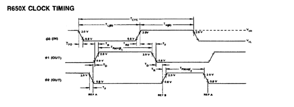
The Electron only produces the phi0 clock on its edge connector. As you can see the phi2 clock looks like a delayed version of phi0. The diagram suggests that the falling edge is slightly delayed and the rising edge is delayed a lot more. I hooked up my logic analyser to by Electron to have a look. The top line is phi0. The lower one is phi2.
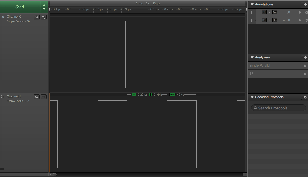
My 100MHz sample suggests that phi2 is delayed about 20 to 30ns on both the positive and negative edges. phi2 is important because the read/write timing diagram for the 6502 always refers to the ‘REF A’ (phi2 falling edge) and ‘REF B’ (phi2 rising edge):
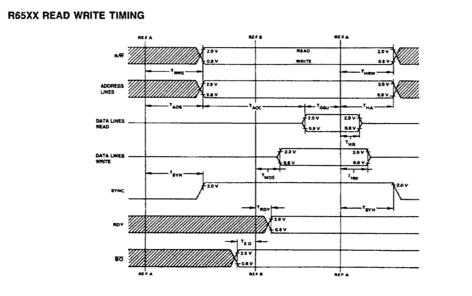
So according to that , in a 6502 write, the databus contains valid data TMDS nanoseconds after ‘REF B’ (ie phi2 falling). My data sheet says TMDS is a max of 100ns on a 2MHz 6502. So relative to phi0 that would be a max of 120ns or so.
The read timing says you should have data on the databus TDSU nanoseconds before ‘REF A; (ie. phi2 falling). My data sheet says that should be 50ns minimum (or about 30ns before the fall of phi0). But the other key thing is THR, the data hold time. You should hold the data for at least 10ns after ‘REF A’. That effectively means at least 30ns after the fall of phi0.
So I had two key changes;
- For a 6502 write, sample the databus a fair way after the rise of phi0. In my case I added a series of NOPs
- For a 6502 read, don’t try to tri-state the bus just after phi0 goes low. Instead ‘hold’ the data for a bit longer. Again, add a number of NOPs.
So all that made a huge difference and the code appeared to work OK on at least two Electrons!
So the way it now works:
- phi0 is connected to PC0 and the negative edge (tail end of cycle) causes an interrupt of the stm32f407. There should not be any other interrupts, so is effectively the highest priority interrupt.
- The ISR routine should kick in around 100ns after the falling edge (optimistically), but it does not do much before going into a polling loop that looks for phi0 going high. That just means we should be able to handle late entry into the ISR and it all still works OK. So this ‘start of ISR’ does things like ‘clear the pending interrupt bit’. To do this quickly and without expending too many clock cycles I’m using some of the floating point registers as ‘globals’. For example, the floating point register s3 has the base address of EXTI, and s1 always has the value ‘1’, so to write a ‘1’ to the pending register I just do:
vmov    r3,s3             // r3 = EXTI

vstr    s1,[r3,PR]      // clear interrupt
So that avoids having to load r3 from a reference in the literal pool or a movw, movt combination.
- So the ‘poll’ for phi0 going high reads port C (phi0 and read/_write are on port C) as well as port E (the address bus of the 6502A) continually waiting for phi0 going high. This way the address bus should be captured around the time phi0 goes high.
- Once we are out of this polling loop we need to quickly establish whether its a sideways ROM/RAM access. If it is then we need to quickly get some data onto the databus of the 6502A so it has time to read it before the end of the cycle. For a sideways ROM/RAM access, phi0 is only high for 250ns. If its a cycle for an IO register then the phi0 high ‘time’ is stretched, so we have more time to service those requests.
So for a sideways ROM/RAM access, it’s always in the range &8000 to &BFFF (ie A15=1 and A14=0). The BASIC ROM is also in that address range, so we need to inspect the sideways ROM select register (&FE05) to work out if it’s a request for a ROM we are serving.If it is a ROM we are serving, we fetch the required byte from the stm32f407’s RAM and turn the D15-D8 pins of port D into outputs so that the 6502A can read the byte. At this point we want to hold data on the 6502A databus until the fall of phi0 (and also a little bit longer).
ARM has a WFE instruction that allows you to pause the processor effectively until an ‘event’ occurs. In our case the ‘event’ is the falling edge of phi0 which we are normally interrupting on. However, because we’re inside the ISR routine, we won’t get interrupted again. But the WFE will allow the processor to continue executing ‘just after’ the falling edge of phi0. We execute a few NOPs since we want to leave the data on the 6502A databus a while longer, then change D15-D8 back to inputs effectively tristating the databus.
So what about if the next cycle is for a sideways ROM/RAM operation? Surely we’ve now just missed the interrupt for it. To handle that we just loop around back to waiting for phi0 to go high. You might think we’d we stuck in the interrupt routine potentially forever, but there are always RAM accesses, and other ROM and IO accesses that allow us to exit the ISR and ‘give time back to the main thread’.
- So there’s other logic ( a branch table) for handling accesses to the peripheral region of the Electron memory space (primarily &FCxx and &FExx). As noted before, the Electron stretches the clock for these accesses which means we don’t need to be so time conscious. There are a few IO registers we handle:
- &fe05 – writes to here update the sideways ROM/RAM select register. For example if you write a 12 here then a ROM/RAM access from &8000-&BFFF needs to select the ROM in ‘slot 12’
- &fc04, 05, 06 07 and &fc0c, 0d, 0e and 0f. These are not part of a Plus 1. If you write a number to any of these locations it asks the stm32f407 board to load a rom from a corresponding directory on the SD card. For example, if you write a ‘2’ to &fc05, the rom file in ‘roms/2’ on the SD card will be loaded into ‘slot 5’.
- &fc70 – writes to this initiate an analog to digital conversion. The Plus 1 has a ADC0884 ADC chip. If you write a 4,5,6 or 7, it starts a conversion for one of the 4 analog channels. Reading from &fc70 reads the current 8 bit digital result of an analog conversion
- &fc71 – This is the plus 1 printer output port. Its deliberately mapped to the SD card pinout used by MMFS. So if you have an SD card connected to the stm32f407 board in the ‘standard SDIO way’, then MMFS will be able to write to it. (I will note here that we’re not actually using the native SDIO support on the stm32f407. MMFS will effectively be using bit banged SPI, and when the stm32f407 talks to the SD card independently, it also will use bit banged SPI).
- &fc72 – This is the Plus 1 input port. Bit 7 is the ACK from the printer, which is used by MMFS as the MISO pin of the SD card. Similarly, Bit 6 is the ‘ADC conversion complete’ pin and Bits 5 and 4 are the fire buttons for the analog joysticks.
- The main thread is a ‘while forever’ loop at the end of main.c. It doesn’t do too much. Essentially there is a way of passing ‘commands’ from the ISR back to the main thread using the ‘main_thread_command’ memory location. The upper bits of determine whether a command is being processed, but then different bits determine what command has been triggered. For example if bit 29 is set then that’s a ‘swap rom command’. Someone must have poked a number into &fc04,5,6,7 or &fc0c,d,e,f so the ‘command’ is to tell the main thread to swap a rom out. The main thread contains its own logic to bit bang the SD card via SPI as well as a seperate FAT32 driver. This ‘swap rom’ command looks at the value written to &fc04,5,6,7 or &fc0c,d,e,f and finds a ROM on the SD card in the corresponding directory under ‘roms’.The main thread also handles analog to digital conversions. In a real Plus 1, you write a 4, 5, 6 or 7 to address &fc70 to start a conversion on channel 1, 2, 3 or 4. You are then meant to poll bit 6 of &fc72 until the conversion completes (since they take a while). So , like the special ROM swap command, a write to &fc70 is passed back from the ISR into the main thread. The main thread then initiates an analog to digital conversion using the stm32f4’s own ADC hardware. When the conversion is complete the result is effectively passed back such that if a read to &fc72 occurs the ADC complete bit is set, and the conversion value is available from &fc70
Using it
There are multiple ways to ‘flash’ a stm32f4 board. There is an example transfer.sh script in the source that shows you how to flash with dfu-util.
Connecting your stm32f407 board is pretty simple. It’s much the same as the previous article. The Electron databus goes to PD15-PD8, the Electron address bus goes to PE15-PE0, and PC0 is phi0, and PC1 is the read/_write line. Full details are on the Github page.
You need to set up an SD card:
- Format it with FAT32. Preferably you should have a small (sub 4GB) partition at the start of the SD card
- Find an appropriate Electron BEEB.MMB on the stardot forums and put it in the root of the SD card.
- Create a ‘boot’ structure to get it to load some ROMs from the SD card on power up. For example, I put the sideways RAM version of MMFS in slot 12, and the AP6 rom in slot 13:
boot/4
boot/5
boot/6
boot/7
boot/12/ESWMMFS.rom
boot/13/AP6v130ta.rom
boot/14
boot/15
- You can optionally place additional ROMs in a different directory structure that allows you to load ROMs adhoc after boot:
roms/1/Hooper.rom
roms/2/Viewsheet.rom
Most games on the Electron will use the keyboard, but the Plus 1’s analog port could allow two analog joysticks to be attached. Per the notes earlier, I do emulate the Plus 1 ADC. You would need to hook up the two joysticks as follows:
PA2 - Joystick 1 X axis
PA3 - Joystick 1 Y axis
PA4 - Joystick 2 X axis
PA5 - Joystick 2 Y axis

PC2 - Joystick 1 fire button
PC3 - Joystick 2 fire button
Assuming the joysticks are simple potentiometer types, the centre pin of each potentiometer just goes to the appropriate PAx pin, and the outer pins of the potentiometers go to GND and 3.3V. For the fire buttons, wire the first one between PC2 and ground. The other between PC3 and ground. You don’t need pullups.
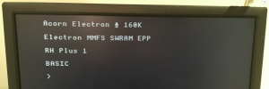
When you power up (assuming you used the same ROMs as me), the Electron screen should look like:
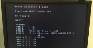
The AP6 ROM has a great *ROMS command to list all the ROMS:
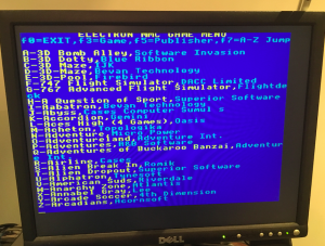
Assuming you have a BEEB.MMB, you can probably enter something like *DBOOT 0 and get a game menu. Here’s the game menu on for the one that I tried:
Source: https://github.com/kernelcrash/electron-rom-emulator
The stardot thread is here.