OK, the Funvision was fun to do on a breadboard, but I thought I’d have a go at a Colecovision. From my distorted view of the early 80s, it’s similar to the Funvision (same video and sound chips), but actually has a lot more chips than the Funvision. More importantly it has a lot more games than the Funvision.
So the basic recipe for a Colecovision is
- Z80A CPU @ 3.58MHz
- 1K of RAM in two 2114’s
- 9929A PAL (or 9918A for NTSC) VDP video chip
- 16K of DRAM for the VDP
- LM1889 colour encoder
- 76489 sound chip
- two 74LS138 address decoders; one for memory, one for IO ports
- An 8K boot ROM
- two 74LS541 buffers that are basically input ports for the two joysticks
- A few inverter chips and NAND gates and other stuff (quadrature controller stuff??)
There are some nice schematics of the Colecovision here. And some technical stuff about the Colecovision hardware at the komkon site. I pretty much used both those resources while building this thing.
The idea was to disassemble much of my Funvision, leaving the 9929A and 16K DRAM stack in place, and hopefully fit it all on the same breadboard setup.
Mods
Per usual, I’ll change the design to suit my needs (which generally means throw stuff out so it will fit on my breadboard).
- The CV (Colecovision) had an interesting clock design. It has a 7.15909MHz crystal , that was divided by two to derive the 3.579MHz CPU and audio chip clock. But then the 7.15909 is also multiplied by 1.5 to get the 10.738635MHz clock that the 9929A needs.For me, I’m just going to use a 74LS04 oscillator setup with a 3.579MHz crystal to feed the CPU and audio chip … and a separate 10.738635MHz crystal for the VDP.
- The two 74LS138’s I will leave much the same, except the CV allowed for some expansion options with some of the inputs to the LS138’s. I will leave that stuff out and save an inverter or two.
- The CV joysticks have both a joystick and a keypad. It is sort of compatible with the atari joystick pinout, but they added a sort of ‘extra ground pin’ for the keypad matrix. That means the CV will drive one of the joystick grounds low to read the joystick and main button, but drive the alternate ground low to read the keypad. They used a couple of NAND gates to implement a flip flop for this. I could have done the same but decided to use half a 74LS74 to do the same thing.There are two 74LS541’s in the CV. One for each joystick port. I only want the one joyport working, so I am only using one 74LS541. Originally I was going to use a 74LS241 or LS244 as I thought I did not have a 74LS541. But I ended up finding one. The 541’s have two output enables, so you need a few external gates if you use a LS241 or 244 instead. Usually the logic uses address line A1 to determine if its reading the left or right joystick, and so A1 or inverted A1 is used as one of the two output enables on each 541. Later I worked out that you can in effect leave out the A1 selection logic and just have the one 541 appear as both joysticks (for single player use, but might work for some 2 player games where you take turns).
One other thing to note about the joystick is that I am using a single button Atari style joystick, so I am limited to games that only use the left fire button. - There is some stuff that connects to p9 of the controller ports (see the schematic) that is to do with quadrature (paddle?roller?) controllers. I’ve left this out.
- I’m using a 512K flash ROM again (29F040). I toyed with a few ways to split it, but to save chips I split it into 64K chunks. That basically means you can only fit 8 games on it. Each chunk is effectively the entire 64K address space of the Z80. But what about the RAM? Yeah, effectively the ROM is always selected for any address ‘except the 8K block from $6000 to $7fff’. So in some ways the memory 74LS138 is a bit useless. Normally, the $0000 chip select goes to the boot ROM and the upper 4 chip selects ($8000, $a000, $c000, $e000) all go to the cart slot.So this all means to build a 64K chunk you need to put the Coleco boot ROM first, pad in 24K of nothing, then put in your cartridge image, then put in padding up to the 64K mark (eg. for a 16K cart, you would pad another 16K on the end of it). I just used dd to create some padding files that I can cat together with the various ROM images. eg. a 16K empty file would be ‘dd if=/dev/zero bs=1 count=16384 of=16KBLANK.BIN’
- The CV put in one wait state during a 3 cycle instruction fetch (M1) cycle. This is most likely to allow longer times for reading atypical slow ROMs of the era. My ROM is going be pretty fast (90ns), so I won’t put in any wait states. This will make it run slightly faster than a real Colecovision, but I am guessing most games hook themselves to the vertical sync pulse so I’m unlikely to see any speed differences (NB: I did end up with a spare flip flop and enough spare gates to implement this logic)
- I still have my 32K cache ram handy, so I am reusing it. Again, A10 to A14 are all tied low so it appears as a 1K RAM chip.
- I’ll use the same DRAM stack and 9929A setup from the Funvision. So a stack of 4164’s soldered on top of each other then wired up to the 9929A but the top address line tied high so that it appears as 16K.
Blink LED test
Per usual, I am just wiring it up to get it to the point of blinking an LED as a first stage test. So the first bit is a few gates of a 74LS04 used as a crystal oscillator. The output goes to the Z80A (p6) and will later go to the 76489 audio chip (p14). Sometimes you may find you have to remove one of the 22pF caps due (probably) to the parasitic capacitance in an atypical breadboard (UPDATE: 2016.02.05 I did this build using an NMOS Z80A. I have since attempted to use a CMOS Z80 and it is much more particular about the clock signal. You might have to ditch the 74LS04 and replace with a 74HC04 with a typical oscillator setup for a CMOS part).
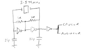
Next I have a 74LS74. One of its flip flops is a simple register that we can use to flash the LED. We’re just feeding D0 from the Z80A and one of the IO port chip selects (see further down)
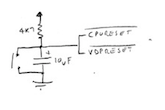
Next is a simple reset circuit with it’s output going to the CPU RESET* input (and later to the VDP chip RESET* input)
Next the Z80A goes in. I used 4k7’s to tie high most of the control inputs; INT*, NMI*, WAIT*, BUSREQ* .
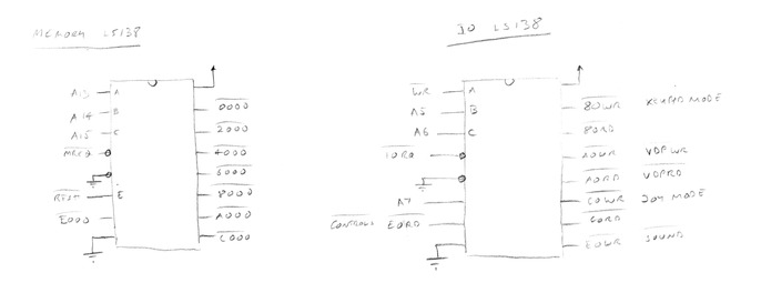
Below the Z80A I have the two 74LS138’s. First the memory decoder one. Next the IO decoder one. I put them in like this which is close but not exactly the same as how the CV does it.
The 80WR* IO chip select will go to our flip flop for our blink test. I’ll note here that the flip flop will be reused later on. This is just for us to do our blink test.
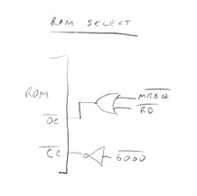
Next is a 74LS32 OR gate. This is not part of the Colecovision at all. This let’s us add a bit more logic to get the chip select for our ROM. As noted earlier its a bit strange. I’m using both the CE* and OE* inputs on the flash ROM (normally I’d tie OE* low). CE* will go low any time the RAM chip enable (6000*) is not low. And to narrow that down a bit, I’m using an OR gate to gate together MREQ* and RD* from the Z80A. There are lots of different ways to do this ‘everything but 6000-7fff chip select’. This was a ‘cheap’ way of doing it for me.
So A0 to A15, D0 to D7 are all wired up between the Z80A and the flash ROM. For the higher ROM address lines I put long jumper wires that I could easily move around, but put them all to GND (ie. A16, A17 and A18)
And put as many 100nF decoupling caps as I could fit around the power lines.
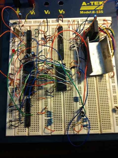
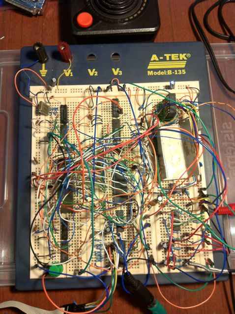
All wired up (on the same breadboard I did the Funvision on) it looks like this. From top left I have the 74LS04 and crystal osc stuff. Next down is the 74LS74 with a red LED just below it. Then I have a reset button it’s resistor and capacitor. Then the Z80A, the memory LS138, the IO LS138. Then in the middle column I have the 74LS32, the 32K SRAM (but its not wired up). Then the Flash ROM. There’s some resistors left over from the Funvision further down and then I just left in the stack of DRAMs and 9929A on the right. It’s not connected up yet.
As per last time, I used a cheap LM2596 based switchmode to supply 5V to the board. Even though the 9929A is not connected at this stage I tend to feed the PSU +5 and GND in close to the 9929A.
I wrote a short blink program and assembled it with asmx. Then flashed the resulting blink.bin to the bottom of the flash ROM (using my Willem programmer).
; Blink LED test
; ./asmz80 -e -w -l -o -s37 -- blinkz80.asm
; srec_cat blinkz80.asm.s37 -o blink.bin -binary

      ORG    $0000000

      ld a,$01
top   out ($80),a
      ld b,a

      ld de,$ffff
loop1 dec de
      ld a,d
      or e
      jr nz,loop1

      ld a,b
      inc a
      jr top
So did it work?
I don’t think so, but I forgot to write down what went wrong. I think it was just an address line in the wrong place. You just need to go over your wiring carefully … and finally I had a blinking LED.
Getting it all running in Black and White
Per the Funvision, the next goal was to wire the rest of it all in and try to get it running in black and white.
So I wired up the 32K static RAM. A10 to A14 are tied low to make it appear as a 1K SRAM. CE* is fed from the 6000* chip select. I have OE* tied low. WE* on the SRAM is hooked up to WR* on the Z80A.
Below the flash ROM I put the 76489 sound chip. It’s important to note that most TI chips from this era had their data buses numbered the opposite way (on TI datasheets) to how other chips are numbered. ie. the D7 of the Z80A goes to the pin labelled D0 (p3) on the 76489. ie. D0 is the most significant bit. D7 is the least significant … so far as TI chips are concerned. The 9929A video chip has the same sort of numbering in its datasheets. Per the CV schematic, the OE* and CE* pins of the 76489 are tied together and go to the E0WR* IO chip select. The READY output goes straight to the WAIT* pin (p24) of the Z80A. You have to tie this high with a resistor (I used a 1K) as the 76489 output is open collector. Make sure the CLK pin of the 76489 is hooked up to the 3.579Mz oscillator. I just put the positive of a 10uF cap hanging off the p7 audio out of the 76489. The negative of the cap goes straight to your RCA for audio out.
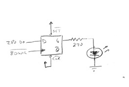
Next is the 74LS541. Originally I thought I did not have a 74LS541 and was working out how I would use a 74LS241 or 244 … but eventually found an LS541. The key difference between the LS541 and the other chips is that the LS541 effectively has two chip enables (both have to be low) rather than one. One chip enable goes to the E0RD* IO chip select. Then you are meant to use A1 to select one of two 74LS541s (in a real CV). One LS541 has A1 tied to it so it’s selected when A1 is low. The other has A1 going through an inverter (ie. selected when A1 is high). For me, I am only putting in one LS541. Originally I just tied A1 to the 2nd chip select … but later I tied it to ground (per the diagram below)… which kinda sorta makes the one controller appear as both controllers which doesn’t seem to be such a bad thing.
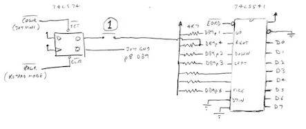
So the output side of the LS541 goes to D0 to D7. The input side has every input tied high with a 4k7 resistor (the Coleco schematic doesnt say what these pullups are … and they are not quite pullups either) except for the D7INput. Originally I had this D7 input tied high as well, and most games would work except for one or two. The D7 input in a real CV is hooked into the quadrature controller circuitry … but its normal dormant state must be low. Some games expect this. I chose not to wire anything (ie. joystick) in to the input side of the buffer yet. My goal was simply to turn it on and see the atypical splash screen that comes up. The diagram above shows an additional flip flop and wiring detail for the joystick as well as a single button labelled ‘1’. At this stage I left all those out.
So next is the stack of 4164’s and 9929A. This is wired up the same as the Funvision. The main things to note about the 9929A wiring are;
- A0WR* goes to the CSW* on the 9929A
- A0RD* goes to the CSR* on the 9929A
- A0 on the Z80A goes to MODE on the 9929A
- RESET* on the 9929A is wired straight into the RESET* on the Z80A
- INT* on the 9929A is wired to the NMI* on the Z80A (yes NMI)
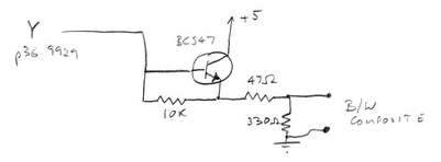
The Y output of the 9929A I wired to a spot below it where I put in the same composite transistor amp stuff that I did for my initial B&W tests on the Funvision (NB: The 9918A, 9928A and 9929A all have roughly the same pinout and at this stage you could pretty much use any of these chips. If you had used a 9918A instead, then this should give you NTSC composite colour output rather than black and white. The 9928A was also for the NTSC market, except it produces separate Y, B-Y and R-Y component style colour output just like the 9929A. The other key thing to note is that the 9918A and 9928A will produce a 60Hz (as per NTSC) vertical sync interrupt, and the 9929A will produce a 50Hz (as per PAL) interrupt. So, in general, games will run slightly faster on the 60Hz chips)
OK, checked everything. Hooked up the composite to a monitor and powered on.
Nothing.
Again, poked around all the wires. I think I had wired A1 to the MODE input on the 9929A. I quickly changed it to A0 and powered on. And it appeared to work;
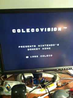
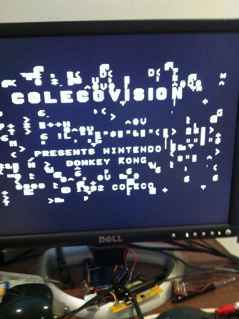
After the notorious ‘pause’ the screen appears that asks you to press 1 for ‘1 player difficulty 1’ etc. I had no way to press 1 at this point.
I thought that was a mild success for the evening so went to sleep.
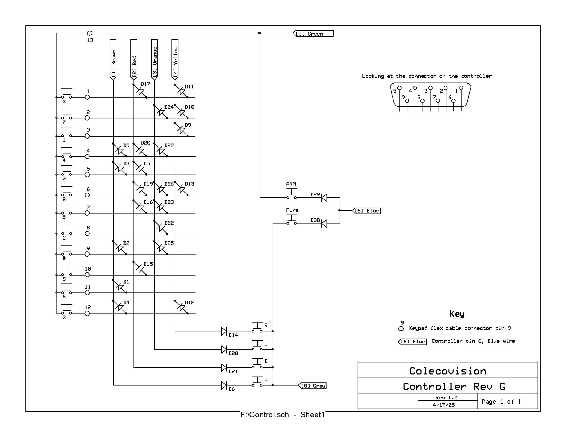
Wiring up the controller
There is a schematic of a coleco controller at the retronicdesign site. I did not have a real coleco controller on me (I returned the ‘family’ CV to my parents house), but I have a few atari style DB9 joysticks which would work in this case. If you look back at the circuit with the LS541 and flip flop you’ll see how I wired the atari joystick in. A key thing is how the DB9 p8 is no longer treated as GND. It is now a strobe line that comes out of the Q* output of the flip flop. The Q output becomes the other strobe. My goal was to be able to press just the ‘1’ key on a Coleco keypad. If you look at that controller schematic you’ll see that pressing 1 would connect p5 (the keypad strobe) to p4 of the DB9. Per my LS541/flipflop diagram I have a push button wired up to bit 1 of the LS541 which happens to also connect to p4 of the DB9. In theory I should have a heap of diodes to protect everything, but I’m just leaving them out for now.
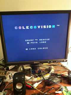
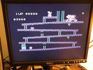
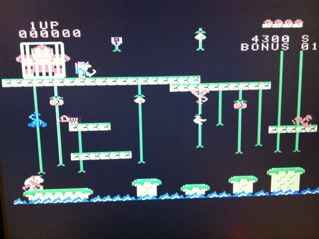
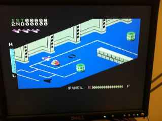
OK, let’s try powering on again. I press my green ‘1’ button at the appropriate time and Donkey Kong starts. I am thinking this is pretty cool.
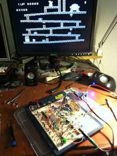
Then two seconds after the Kong rolls his barrel, it reboots and I am back to the splash screen. Sometimes I get garbage on screen like so when it reboots. Othertimes it reboots cleanly. Sometimes it reboots as soon as Kong appears. Othertimes a few seconds pass.
I try a few more games, and they all have very similar behaviour; splash screen appears, press ‘1’, I see the initial screen of the gameplay … but then it reboots.
I scratch my head a bit. I check my wiring again. I swap out the Z80A for another Z80 I had. No change.
I then start to think about how important it was in the Funvision to fake a ground plane to remove much of the interference from the video output. Maybe the ground between the CPU and the 9929A is a bit crap.
So I tried running a jumper wire from the GND pin of the Z80A to the GND of the 9929A. And that made it work!!!! I tried a few of the games. Most seemed to work (though Miner 2049er crashed … but later on when I tried to beef up my ground plane even more it started working). I think this whole project has taught me the importance of a decent ground plane. In hindsight, I think it is a better choice to put the CPU as close to the video chip as possible to make it a short path to tie the grounds together. ie. I would probably put the Z80A in the middle of the breadboard design next time.
Colour
So my B&W testing was all good at the moment, so then I pulled out the composite video transistor amp and wired up the LM1881, 4066, transistors, resistors and caps that I set up for my last attempt at component video on the Funvision. Here it is all wired up. The colour circuitry is directly below the 9929A. If you look closely I have a heap of jumper wires all going to very close to each other in the GND line on the right edge of the board. This is then jumped back to the 9929A GND. I also have jumper wires that tie together the GNDS at the bottom of the board (you’d think this would not make a difference but it does when you are trying to diminish onscreen interference. This is the kind of thing you can play around with a lot. You may also find moving the ground wires of the connections you have to your component video cables can help. I had a case where I had quite severe vertical line interference and the ground to the Y output was on the far right per the picture … but moving the ground lead to the other ground bus, in line with where the 9929 has its ground pin made a world of difference).
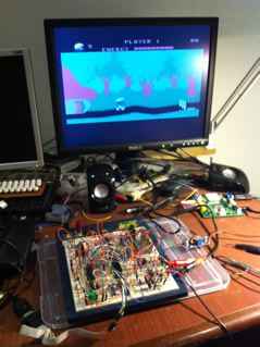
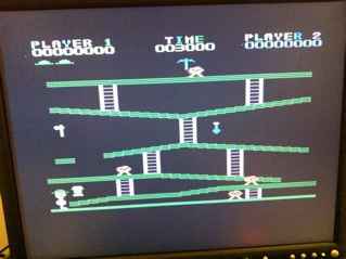
And here’s some pics. Looks generally better than composite output I was getting from a real Colecovision. As per my article on colour, its still a bit of a hack and has a blue-ish tone to it and the yellows are still a bit washed out.
Squeezing more games into the ROM
So, using 64K chunks in the 512K ROM limits you to 8 games total. I thought there must be a reasonably easy way to use 32K chunks somehow which might give you 15 games (15 plus one extra one for the BIOS ROM). I originally tried some scheme where I swapped out the memory LS138 for a 74LS157 mux and had the CPU A15 line tied to this mux. The A inputs of the LS157 were all tied low, and the B inputs went to 4 jumpers I could tie low or high. The output of the LS157 went to the top four address lines of the 512K ROM.Then I used some spare inverters and OR gates to make up some chip select logic (since I removed the LS138 for decoding memory addresses). So the idea was that you put the BIOS in the lowest 32K chunk of the flash rom, then put games in the remaining fifteen 32K chunks. When A15 is low, the mux forces all the top ROM address lines low to address the first 32K chunk. With A15 high, one of the other fifteen chunks is addressed depending on your jumper settings. Sounds reasonable?
It never worked. Well, it worked a bit but exhibited all the bad symptoms of the ground plane being stuffed. A game would appear to start, then 2 or 3 secs into the game the computer would reset. I scratched my head a lot trying to get it to work.
But I gave up and tried a different approach. So I keep the 74LS138 that decodes memory, and that one OR gate I used, well I now use all four OR gates per the diagram below.
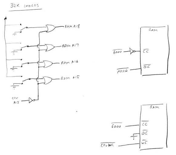
So you still have the jumpers (shown as switches) now going to one side of every OR gate. The other OR gate input is driven by the inversion of A15. So when A15 is low, the inverter sends a high to every OR gate which will force the outputs to also go high. Hence the BIOS ROM needs to be in the last 32K chunk of the 512K ROM (address $78000). When A15 goes high, whatever is set using the jumpers is passed through to the Flash ROM, so setting 0000 on the jumpers picks the first 32K chunk of the ROM, 0001 the 2nd 32k etc.
And this all works. I’m still not sure why the use of the 74LS157 caused so many problems.
The one OR gate I was previously using to generate the OE* for the FLASH ROM is now reused, so I am just running MREQ* to the OE* on the flash ROM.
(UPDATE 20160211) : Breadboards
I have a friend interested in making one of these … so long as it came as some sort of ‘kit’. Taking that as a bit of challenge, I set out to make another breadboard Colecovision and take lots of photos to make some decent instructions. I thought I would change the parts list a bit, since some items are hard to get, namely
- Instead of my 30yr old A-TEK breadboard I bought some of the MB-102 breadboards that you see all over ebay/aliexpress for roughly $3 each.
- Use a CMOS Z80 instead of a NMOS one
- Use a 21.47727MHz crystal divided by two to derive the video chip clock.
Now these MB-102 breadboards I don’t particularly like since wires never seen to fit very tightly in them, but I thought ‘everyone on the internet seems to use them. They must be OK’. So I built it in stages again. I had some trouble at the blink the LED stage as the CMOS Z80 needs a nice clean clock signal, whereas the NMOS one tolerate a rough one. I figured that out, then built the rest of the system on three of these MB-102 breadboards. It did not work at all. The video section is very sensitive to voltage droop and the lack of a decent ground plane. I eventually got it partially working but at times it was like the breadboard was not conducting electricity at all. It was a puzzle.
As an experiment, I found another 30 yr old breadboard. It had gone yellow in the Australian sun, and sounded very rusty when inserting wires, but wires fit very tightly compared to the MB-102 boards. I was on the virge of throwing the yellow board out many times over the years because it looks like some animal peed on it, but thought I would try it here. So I put the 9929A and DRAM stack from the MB-102 and put it on this really old breadboard (possibly Wish brand as it has a ‘W’ on it) and the Colecovision now works perfectly.
Having bought a few of these MB-102 breadboards I am realistic that 1) for a lot of slow applications with a few chips they are fine and 2) that once upon a time some manufacturer made a really high quality version of these MB-102 things, then several Chinese manufacturers all cloned it, and tried to cut costs where possible, then cloned these again and tried to cut costs … until you have the world of today where you can’t tell if they are actually decent quality or not. I am sure ‘some’ of these MB-102 things are decent … but I have no idea which ones.
Anyway, I’ve ordered some more expensive ‘name brand’ breadboards from Element14 hoping that these will be of decent quality .. and I will continue on with this ‘kit’. Anyway, I’ll undoubtedly have another article when I finish this off … and here it is