The Texas Instruments TI-99/4 came out in 1979, and had some minor updates to become the TI-99/4A in 1981. Texas Instruments has seemingly been around ‘forever’. They make a lot of things, but just like today they made a lot of semiconductors in the 1970s and unsurprisingly the TI-99/4A has a lot of ‘TI’ chips in it. In that same ‘late 70s/early 80s’ period quite a lot of home computers were released. Most would have had 8 bit 6502 and Z80 CPUs, but the TI-99/4A had TI’s own TMS9900 16 bit CPU. It also had TI’s TMS9918 Video chip with 16KB of ‘Video RAM’. I always liked the TMS9918 (or TMS9929 in the PAL world). It was in the Colecovision, Dick Smith Wizzard/Funvision, Sega SC3000 and all the early MSX machines. The ‘usual configuration’ is to have it hooked up to 16KB of dedicated DRAM. So far this all sounds good. But strangely the TI-99/4A has only 256 bytes of RAM for the CPU and a fair chunk of that is used for ‘register storage’ as the TMS9900 had the unusual idea of putting registers in RAM (I’ve seen references that this idea comes from the minicomputer tech back then). Having registers in RAM means you have a lot more RAM accesses compared to other CPUs of the era.. It runs at 3MHz, and there are wait states inserted , and additionally the internal 16 bit bus gets converted to an 8 bit bus when accessing the cartridge slot or the I/O expansion (so at least two cycles to access anything). In addition it has this ‘read before write’ architecture which means that any write to memory is always preceded by a read first.
So it’s not the fastest thing in the world, but it is very interesting, and like a lot of machines of the era clever people figured out ways to push them.
And so yes I recently acquired one (again, many thanks to the same reader that I acquired the Coco 2 from).
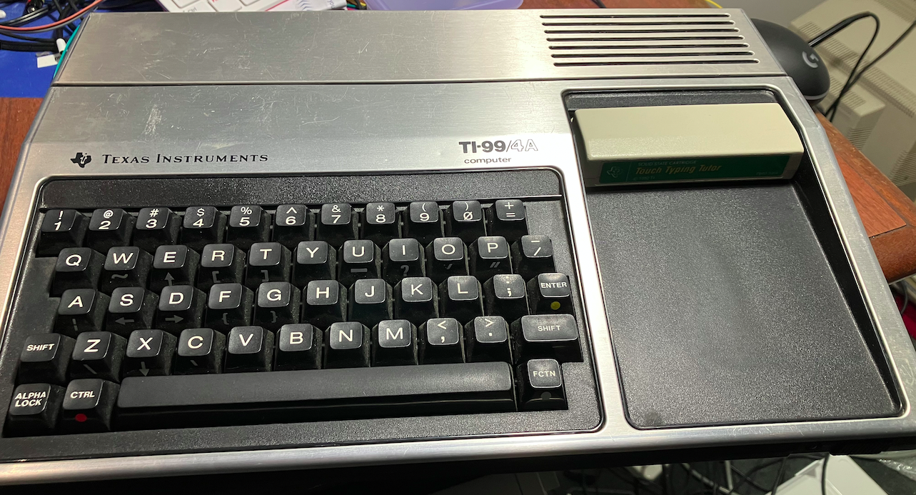
It’s a nice looking little machine. It has a nice mechanical keyboard (though I thought I read that TI changed keyboard vendor throughout the production run). On the top to the right of the keyboard is the cartridge slot. I think this is sometimes called the ‘Module slot’ or the ‘GROM port’. On the right of the machine is the IO port, which is the main expansion port. Around the back you have what looks like an Atari joystick port but its actually the cassette interface port. There’s also a power connector, and then on the far side at the back is a DIN port for video and audio out. Then on the left hand side you have another port that looks like an Atari joystick port … and I thought surely this must be the joystick port. It is the joystick port. However it has a different pinout to the standard Atari joystick, so I had to make an adapter up. It’s actually designed so that you can plug two joysticks in to the one port.
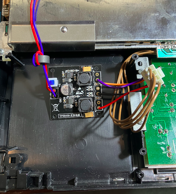
Just like the Coco 2, I did not have a power supply. This is a NTSC TI-99/4A as well, but I didn’t need to worry about 120VAC. It would have had some external ‘power brick’ back in the day. The same reader had mentioned some cool DC-DC supplies on aliexpress based on the TPS5430. For my purposes these take a +12V DC plug pack as input and produce both +5V and -5V. The TI-99/4A just happens to need +12V, +5V and -5V. I removed the internal switchmode PSU board and replaced it with with one of these TPS5430 boards and I had a working TI-99/4A!
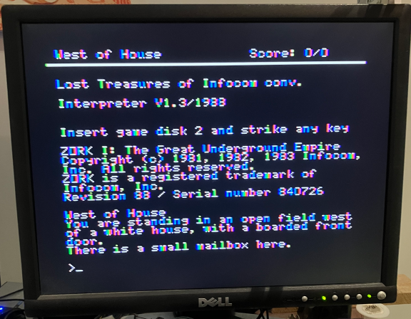
I only had a ‘Touch Typing Tutor’ Cartridge to play with, but the video quality is really good for composite NTSC.
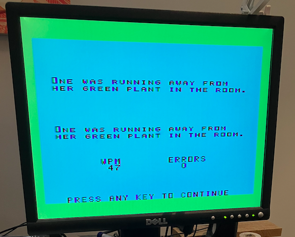
The TI-99/4A does come with a built in BASIC interpreter like most machines of the era. As I was to learn later, this ‘built in BASIC’ is not so awesome and everyone just uses one of the ‘TI Extended BASICs’ that are out there. It’s interesting that there is a BASIC at all given there are only 256 bytes of CPU RAM, but like some other machines with the TMS9918/28/29 video chip, your BASIC program was actually stored inside empty space within the 16KB of Video RAM.
Anyway, there is not a lot you can do with the ‘not as awesome BASIC’ and a Typing Tutor cartridge, so naturally I decided I would build a ROM and Floppy Disk emulator using an stm32f407 board 😉 .
So began a mountain of research as this machine is quite different to anything else from this era.
So there are already some ROM and GROM emulator cartridges out there already. The main ones that caught my eye are the FlashROM99 and the FinalGROM99. FlashROM99 emulates ROMs, and the FinalGROM99 emulates ROMs and GROMs.
So what the hell is a GROM? One of the most useful sources of TI-99/4A info is Thierry’s TI-99/4A tech pages. He has a really informative page all about GROMs. Essentially they are a sort of ‘serial ROM’ that TI came up with. Unlike a normal ROM or EPROM where you have a full binary address bus and an 8 bit data bus. the GROMs basically just have one address bit and an 8 bit databus. If you’ve ever written software to program the TMS9918/28/29 chips you will recognise the programming interface. You essentially load an address register inside the GROM, then read bytes out one by one and the internal address register auto increments after each byte. TI sold lots of cartridges that seemingly had a ROM chip and maybe a GROM chip or two (I am happy to be corrected on that, as I am just going on the contents of cartridge dumps). You could have up to five 8KB GROMs in a cartridge (even though not all 8K is useable) alongside one or two 8KB ROMs.
So the GROM slot on the top of the TI-99/4A is a 36 pin edge connector. There are control signals on this connector for connecting ROMs and GROMs. The address pins for the ROM are limited to 8KB alongside a chip select signal for 0x6000-0x7fff which is the standard location for ROMs. In order to use ‘more than 8KB in a ROM’ various bank switching systems were created … and there are a few. The most common involves a latch that picks up writes to 0x6000-0x7fff and latches those as upper address bits. In its simplest case this involves latching two address lines to become two upper address lines to the ROM, and hence you can have a 32K ROM attached. This is generally how the flashROM99 works (there are at least two versions of this latching design. One where the latched address lines are inverted, and another where they are not inverted). Without going in to detail, the modern TI-99/4A ‘community’ have worked out ways to convert a game that used ROMs and GROMs to one that might instead fit within a single 32K ROM.
So my first goal was to emulate a simple ROM in the GROM slot. Using the dragon-rom-and-floppy-emulator as my starting point, and with my logic analyser handy I soon discovered the beginnings of a rabbit hole. Now that I’ve done this sort of ROM emulation a few times you get used to CPUs where they ”get some address on the address lines’, then ‘assert some memory access’ signal (eg. _MREQ on a Z80) and a read/write type signal and then expect a ROM to shove some data on the databus a ‘reasonable amount of time’ before the memory access signal finishes. The expectation is that the address lines will be stable throughout the memory access cycle. The TI-99/4A is not like this.
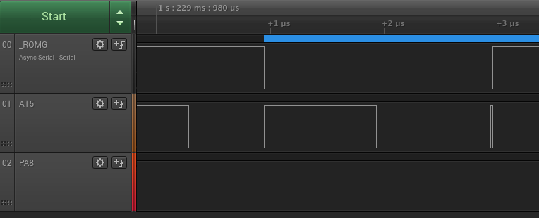
The TI-99/4A puts an address on its data bus with the lowest address line (A15) high, then asserts the _MEMEN signal and then assumes a ROM would present data within a reasonable time period, but then instead of the _MEMEN going high to end the cycle, A15 goes low part way through the cycle while _MEMEN remains low. A normal ROM chip would then obviously switch itself into presenting the byte with the changed address within a reasonable time period. Eventually _MEMEN does go high … but it’s quite odd. In the GROM port you get the _ROMG signal. It’s the 0x6000-0x7fff chip select … which is effectively _MEMEN per the previous discussion. You can see below on this logic analyser trace how A15 goes low half way through. The other thing to note is just how long one of these memory cycles are. There are quite a few wait states in there and the whole thing is roughly 2us for this ‘grab two bytes’ access.
I’ve had cases where the _MEMEN cycle seems to go even longer. I haven’t seen this mentioned in any of the doco I’ve read, but suffice to say I had to take a different approach when emulating a ROM chip. I took the approach of
- Interrupt the stm32f407 on the negative edge of _ROMG
- Grab the address bus of the TI-99/4A
- Look up a data byte to present
- un-tristate the data bus
- Output the data byte
- Check if _ROMG has gone high. If it hasn’t then loop back to step 2 to pick up any address changes.
- If _ROMG has gone high then exit the interrupt routine.
I usually don’t like ‘looping around’ inside an interrupt service routine as its not fast … but in this case the TI-99/4A is not that fast so we have time to waste so to speak.
I’ll mention here a few good sources of info related to TI-99/4A bus cycles; The TI-99/4A Console and Peripheral Expansion System Technical Data, Thierry’s page on the TMS9900 and the TI-99/4 New Technician Guide 001-080 and the 2nd part TI-99/4 New Technician Guide 081-156 .
So that was enough to get me an 8K ROM based cartridge to start. Next was to implement the logic to simulate the ‘latch’ that allows you to bank switch up to 32K in a ROM. That was problematic as ‘writing to memory’ is a sort of weird special case because it will appear that the TI-99/4A is doing a read cycle before a write cycle per this ‘read before write’ archtitecture. That is a little strange, but then I thought the TMS9900 has no ‘Upper data strobe’ and ‘lower data strobe’ signals like a 68000 has so that it can do byte addressing, so the TMS9900, in order to write to a byte, needs to read a 16 bit word from memory first, then change either the upper or lower byte then write the entire 16 bit word back. So even though that is slow, it does kind of make sense, but I read a comment on the atariage ti994a forums that indicated that the TMS9900 does this read before write on 16 bit word writes as well!
I have to mention this before I continue on. If you’ve used a TMS9918/28/29 and looked at TI’s data sheet you’ll know that the data bus pins are the opposite way around to how ‘everyone else does it’. So instead of D7 being the most significant bit and D0 the lowest, TI has D0 as the most significant bit and D7 as the lowest bit. So the TMS9900 has this same logic applied to the address bus. A0 is the most significant bit and A15 is the lowest one … even though A15 is not a real address pin. A15 is generated in hardware to allow for the byte addressing that takes place when the 16 bit bus of the TMS9900 is multiplexed to become an 8 bit bus. This all sounds simple enough until you start looking at circuit diagrams and try to convert the address pins in your head.
As soon as I had ROM emulation running, I soon discovered that many of the ROMs that worked with the FlashROM99 required the ’32K RAM Expansion’. I did not have such a thing. I assume this ’32K RAM expansion’ was popular as quite a few things depend upon it. It makes logical sense that you would want to go from 256 bytes of RAM to 32K and a bit. The stm32f407 board has spare RAM so I could easily make it emulate the 32K RAM Expansion … but I immediately realised that it’s not possible via the GROM port. The chip selects and/or additional address pins are just not present. They are present on the side IO port connector.
I then scrapped the idea of connecting the stm32f407 to the GROM port and wired it up to the IO port instead. You don’t have the _ROMG signal anymore, but you get _MEMEN and the full address bus, so my code now interrupts on every _MEMEN going low, checks the upper address lines and does what it needs. Adding the 32K expansion was not that hard, though its mapping is odd; there is an 8K block at 0x2000-0x3fff and then the remaining 24K is at 0xa000-0xffff. I had more fun getting ‘writes’ to work correctly as it is a ‘special case’, but i was able to play all the FlashROM99 games that need the 32K RAM Expansion.
Next on my list was GROM emulation. Effectively the interface to all GROMs is exposed on only 4 addresses ; 0x9800, 0x9802, 0x9c00 and 0x9c02 . I needed an ability to write to an imaginary address register and to auto increment after each read. Again, ‘writes’ were even more problematic here as you cannot accidentally write twice quickly to the address register, otherwise the address will get messed up. My workaround is really to watch the _WE signal once it goes low … and to avoid rechecking the address bus until it goes high. There is a function of GROMs where the TMS9900 can read the content of the address register (actually it reads the address register plus 1), but I found that was not used by anything so I have left that out.
And so I now had GROMs working. There are a few different cartridge dump formats for the TI-99/4A, but many will show files that end like so
- Files ending in C.BIN which are usually 8K
- Files ending in D.BIN which are usually 8K
- Files ending in G.BIN that could be up to 40K
So the ‘C’ and ‘D’ files are really just two banks of the 8K ROM space. The ‘G’ file is one or more GROMs concatenated. Some cartridges have ‘just a C file’. Some have a ‘C and D’. Some have a ‘C and a G’. Some have a ‘C, a D and a G’. Some emulators like ti99sim and MAME group all these files into a single file (like a .ctg file for ti99sim). I assume this makes it easier for someone who ‘just wants to run a game’.
So that got even more cartridges working OK.
Floppy Disk Emulation
So onto the next challenge ; emulating a Floppy Disk Controller and disk. Here is where I got confused early on. I found a schematic of a TI-99/4A floppy disk controller card. It had a FD1771 floppy disk controller chip, two 4K ROMs and some other logic and I thought ‘this must be the one’, but eventually I realised it is ‘some other FDC board that is very similar’. I am honestly not sure which TI model number it is. Later I realised the ‘Floppy Controller card with the PAL’ is probably the PHP1240 Floppy Disk Controller card that is the more common one. Again, Thierry has a TI Disk Controller card part 1 and TI Disk Controller card part 2 that go into some detail.
So the FD1771 belongs to the same family as the WD2793 etc that is used by lots of other computers from this era, and of course the Dragon rom and floppy emulator I had recently worked on uses one of these chips.
The first gotcha with the FD1771 is that the databus is inverted. It barely rates a mention in the FD1771 datasheet.
The FD1771 needs 4 addresses generally, but in the case of the TI-99/4A it maps to 8 addresses so that the reads are on different addresses to the writes (I assume this is to get around the problems of the read-before-write architecture). You basically have this mapping.
5FF0 – status read
5FF2 – track read
5FF4 – sector read
5FF6 – data read
5FF8 – command write
5FFA – track write
5FFC – sector write
5FFE – data write
So the FDC chip does not always appear at these addresses. The TI-99/4A has a sort of peripheral memory region at 0x4000-0x5fff called the DSR space (I think). So that is an 8K block and a normal TI FDC controller card has 8K of ROM that appears at 0x4000-0x5fef (ie. the last 16 bytes of address space are diverted to the FDC chip). But again, it only appears at these addresses when the FDC is ‘enabled’.
And so how is the FDC enabled? This is where the TMS9900’s CRU bits come in. Again, Thierry has a page all about CRU. Its like a bit setting/resetting and reading interface. For an output operation, the TMS9900 has instructions such as SBZ (set bit to zero) and SBO (set bit to one) where effectively one of 4096 possible bits is set or reset. Per the TMS9900 manual:
The TMS 9900 utilizes a versatile direct command-driven I/O interface designated as the communications-register unit (CRU). The CRU provides up to 4096 directly addressable input bits and 4096 directly addressable output bits. Both input and output bits can be addressed individually or in fields of from 1 to 16 bits. The TMS 9900 employs three dedicated I/O pins (CR UI N, CRUOUT, and CRUCLK) and 12 bits (A3 through A14) of the address bus to interface with the CRU system. The processor instructions that drive the CRU interface can set, reset, or test any bit in the CRU array or move between memory and CRU data fields.
When the TMS9900 is setting or resetting one of these 4096 bits it puts out which bit to change on the address bus (excluding the most signification 3 bits), and then the CRUOUT pin (which is also used for A15 on the IO port) is either low or high depending on whether its a clear or set operation, and then CRUCLK is pulsed low briefly. Reading a bit is similar in that the TMS9900 outputs an address, and then reads on the CRUIN pin to work out whether that CRU input is a 0 or 1. There’s no specific signal to say this is happening, which I realised could be a problem for me, but more on this later.
The main important thing is that the Floppy disk controller and its ‘DSR ROM’ is enabled when there is a set (like SBO) to the CRU 0x1100 address, and disabled for a clear (eg. SBZ) to 0x1100. Obviously my system emulation would need to look for these CRU ‘writes’. When looking at the timing diagram for CRU writes, the CRUCLK is shown as going low very briefly. The data sheet says for a ‘minimum of 80ns’, but it also shows the address bus as stable either side of this short pulse. Given I was going to use an interrupt driven design and interrupt on the negative going edge of CRUCLK, the first line of any Interrupt Service Routine (ISR) is going to be at least 100ns from that edge, so if it really was 80ns, I would miss the low period of CRUCLK and be sampling the address bus just after it went high …. which ultimately I thought is fine and probably would not be a problem … and it turned out it wasn’t a problem. Later when I hooked up my logic analyser I could see CRUCLK going low for about 160ns which is even better for my design.
There are a few other CRU bits used for outputs. Things like side select and disk select signals for up to 3 drives. An interesting one is the bit to control whether wait states are inserted. On Thierry’s pages its describes what happens to the INTREQ and DRQ outputs of the FD1771:
INTREQ and DRQ are ORed together and with the inverted motor strobe then go the the D input of a 74LS74 D-flip-flop clocked by the CLKOUT* bus line (buffered by a 74LS244) and cleared by the CS* signal from the custom control chip, via a 74LS04 inverter. The Q output clocks a second 74LS74 whose D input is pulled-up (also cleared by the inverted CS* signal) and whose Q output is ORed with the (non-inverted) CS* signal from the custom IC and CRU bit 2 inverted by a 74LS04. The resulting output is inverted again by a 74LS04 and enabled a 74LS125 buffer whose input is grouded and whose output controls the READY bus line. Got that?
Yeah, I didn’t understand it either ;-). But effectively that ‘bit 2’ (or 0x1104 in the CRU map) can control whether the TMS9900 gets wait states when it tries to access the FDC chip. It’s a bit like how the Tandy FDC controller would drive _HALT low, and hence allow a program to read or write a sector from/to the FDC data register without having to check if the FDC is ‘ready’ for the next byte. I think I worked out that the way the TI-99/4A does it is sort of the opposite way around to the Tandy, but more importantly I worked out with my implementation that simply ‘not caring about it’ actually works. ie. Don’t bother to drive READY at all. As my FDC emulation simply loads an entire track into RAM on the stm32f407 after every seek, it means that you can read or write a sector as fast as you like. Anyway, I did not need to do anything with the INTRQ and DRQ stuff at all this time round. My code still sets and resets them where a normal FD1771 would … but they are not used at all.
What about CRU inputs? So my implementation has interrupts on the _MEMEN and CRUCLK signals. CRU inputs I thought would be hard to do properly since there is no ‘easy’ signal to work out that a CRU read is happening. But I was hoping they were rarely used. It turns out they are only really used once in early drive initialisation. There are 3 CRU inputs that match the 3 CRU disk select outputs. During initialisation each of the 3 disk select CRU outputs is sent low, and the corresponding CRU input bit is read back. If it also reads low then it means that a drive is attached. So, if you only had one drive on a real TI-99/4A it would read back a low when you pulsed the DSK1 CRU output low, but when DSK2 and DSK3 were pulsed low , the TMS9900 would read back a high for DSK2 and DSK3. I had a theory that if I simply pulled the CRUIN pin low with a resistor it would generally read a low and hence fool the FDC initialisation code into thinking there were 3 drives attached. Again, this turned out to actually work. You can program the stm32f407 to have a pull down on GPIO pins, but they are quite weak pulldowns. I found that simply attaching a 3.3K resistor to GND on CRUIN made it all work. Later I worked out that you could achieve the same thing with a one byte patch to the FDC DSR rom. I’ll note here that I used the FDC DSR rom called DISK.BIN with an md5 of 3169cfe66687d5b9ed45a69da5a12817.
So after many late nights I had the disk interface working with a simple push button interface (like in my other designs). I had a NEXT and PREV button to cycle through items in a directory on an SD card. I had to take a different approach to my other designs. Instead of just dumping ROM and disk images into a single directory on the SD card, I have the “ti994a” directory on the card containing subdirectories for each game. Those subdirectories can contain a .dsk image as well as any related C, D and G files. I found with the TI-99/4A that disks especially often have a dependency on a particular cartridge or group of cartridges. For example, there are lots of disks that will autoboot so long as you are running off an ‘Extended Basic’ cartridge, so in order to boot the disk version of ‘Pitfall’ I would place the Pitfall .dsk image and the C, D and G files for Extended Basic in the same directory (I will note here that I had most success with Extended Basic 2.5. More to the point, the V100 one did not work at all with disks). Some subdirectories would just have a C and a G file, or just a G file and so on. I also had a mechanism to load in the 8K DSR rom for the Floppy Interface as well.
Initially I just emulated access to the 40 track, 9 sectors of 256 bytes per track raw .dsk images that seem relatively common in the TI-99/4A world. These are the .dsk files that are 92160 bytes long. There are a couple of other image types as well. Another one I wanted to do was Two sided, 40 track, 9 sectors of 256 bytes per track. These files are 184320 bytes long. I’ve added code for handling double sided disk images in my other emulators so I was expecting this to not be hard (well, excluding all the problems I had with trying to get OS-9 and NitrOS-9 going on the Coco 2). Most other disk images for retro systems will interleave the 2nd side track data in the file. So in the case of the TI-99/4A it has a track of 9 sectors of 256 bytes . ie. 2304 bytes. I assumed in a double sided disk image the first 2304 bytes was track 0, side 0, then the 2nd 2304 bytes was track 0, side 1, and the next 2304 bytes was track 1, side 0 and so on.
That interleaved track setup did not work, so I actually tried to find some documentation and read the source of other emulators. The first thing I read is that all the 2nd side tracks are in the 2nd half of the disk image file, so the first half is tracks 0 to 39 side 0, and I assumed the second half was tracks 0 to 39 side 1. This turned out to be a bit wrong as well. It turns out that track 0 side 1 is the 2304 bytes at the very end of the disk image. Then track 1 side 1 is the next 2304 bytes in from the end of the disk image file and so on. So track 39 side 1 ends up sort of being in the middle of the image file.
I was almost going to stop there for the disk support. But I was trying to play Zork 1, and realised that trying to save to a save disk was going to be difficult. In my other emulators I’ve forced the user to press the NEXT and PREV buttons to simulate ejecting and inserting the save disk. I realised that that might indeed work, even using the subdirectory setup, but it would probably be annoying. Much nicer would be multiple disk support. In the past I’ve avoided multiple disk support as it creates a lot of potential failure scenarios … which means a lot more testing. Anyway, I ended up adding support for 3 disks. If you just put a file ending in .DSK or .DSK1 into the relevant subdirectory then it will be used as DSK1. If you put a file ending in .DSK2 then it is used as DSK2, and logically a file ending in .DSK3 is treated as DSK3. I’d suggest making sure all the disk images are the same size (ie. make sure all the disk images in a subdirectory are 92160 bytes, or all of them are 184320 bytes).
A Menu Interface
So my previous designs have generally had some simple menu interface (KCDFS/KCTFS for the Dragon and Tandy). These are always native programs on the system in question that communicates through a few IO or memory addresses to the stm32f407. For the TI-99/4A this meant venturing into the world of TMS9900 assembly language. Another rabbit hole. When I first started looking at it, it looked completely alien to me. I’ve done plenty of 6502, Z80, 68000 and x86 coding, but the TMS9900 stuff just looks weird.
MOV 3,3
JNE >03AA
LI 1,>0005
CLR 2
This is actually one of two main syntaxes I think. The example above is the one where the register names are missing ‘R’ to say they are a register. You can rewrite the above to the other main syntax:
MOV R3,R3
JNE >03AA
LI R1,>0005
CLR R2
That makes it a little more readable. MOV is a move instruction. It has some cool address modes, but this first one is just moving register 3 to register 3 which is basically just to set the flags. Registers are 16 bits. The JNE is a ‘Jump Not Equal’, but its a relative branch (like a BNE), and then the symbol that confused me for ages ‘>’ which is just the symbol for a hexadecimal number! Doh! So that is address 0x03aa. Next is an ‘LI’ which is ‘Load Immediate’ (this all reminds me a little of RISC-V assembly), so that’s load immediate register 1 with 0x0005. CLR R2 is just ‘set R2 to zero’. I looked at a few ‘Assembly language for TI-99/4A’ type books from back in the day and they were OK, but one site that I found really handy is the ChibiAkumas TMS9900 page. The colours might look a bit weird to some people, but I quite like it. It sort of explains things in terms of ‘you probably have experience on some other assembly language’. It even has a handy TMS9900 cheatsheet showing instructions and opcodes.
There’s some unusual bitwise instructions and even multiply and divide.
I’ll mention here too a few other points:
- So most of the registers are in RAM. The only ‘true’ registers are the PC, flags and the ‘Workspace Pointer’ (WP) which is basically a pointer to where you want your 16 registers to appear in RAM.For example, if you set the WP to 0x8300, then R0 is 0x8300 and 0x8301, R1 is 0x8302 and 0x8303 etc.
- There is no stack. You are meant to shuffle a register around and handle nesting yourself.
- It’s a big endian processor (like the 68000, but not like x86).
- The MOVB instruction is for ‘move byte’ but when you move to or from a register, then it always uses the high order byte of the register.
- The RESET vector is not just a simple 16 bit address. First it is the 16 bit Workspace Pointer value to assign, and then the 16 bit address to jump to.
I ended up using the xdt99 cross development tools . This includes a TMS9900 assembler written in python. It’s quick and there are some good simple examples with it. That was enough to let me work on a simple menuing program.
One of the first things I noticed is that the default character font at boot time is uppercase only and the characters extend all the way to the edges of the 8×8 characters cells. This means if you put two lines of text one on top of another, its very hard to read since the bottom of the first line merges into the top of the 2nd line. Initially I wrote the new KCTFS menu program to only output 10 lines of entries per page, leaving a blank line between each, but I eventually decided it was better if I just uploaded a better 8×8 character set and used that instead. It is still uppercase only, but it allows me to cram 20 entries per page. Here’s an example. It does the job. Currently you can have up to 9 pages of 20 entries.
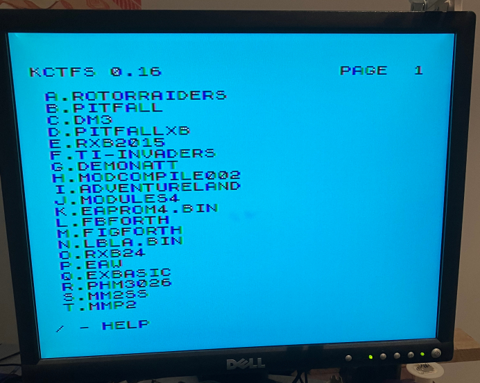
You just press a letter, and the ROM/GROM/disk combination you want is loaded and the TI-99/4A reboots. Then when you get to the main screen where it lists “1. TI Basic” , it should have the selected game or app as option 2 (and some games have a 3 and a 4 and so on).
To switch games, there is a MENU button. It resets the loaded ROM back to the KCTFS menu. Ideally you press the MENU button when you are NOT executing a ROM or GROM. My usual approach is
– press FCTN = to try to reset the TI-99/4A. This amazingly works in a lot of games, but there are many where I need to unplug power and replug power to the TI-99/4A (if I had a proper reset button this would be easier).
– press the MENU button on the “Press a key” screen.
– press FCTN = again to reset the TI-99/4A
– “Press a key” and you should see KCTFS as option 2. Press ‘2’.
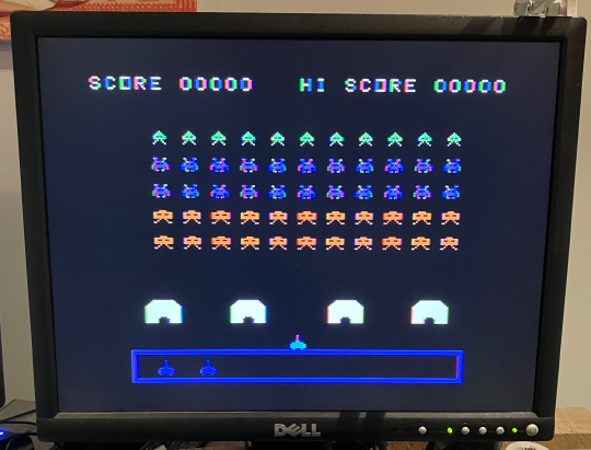
So what works?
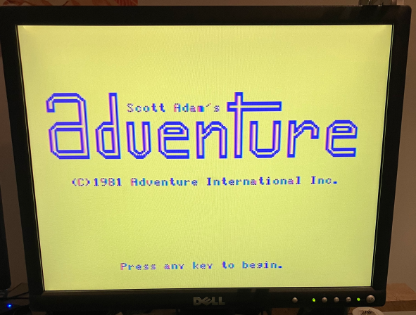
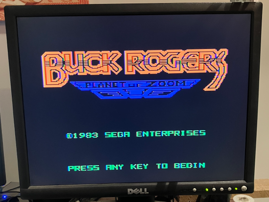
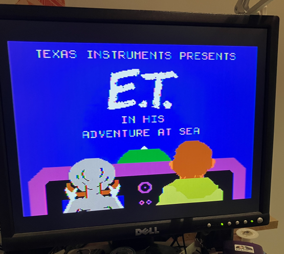
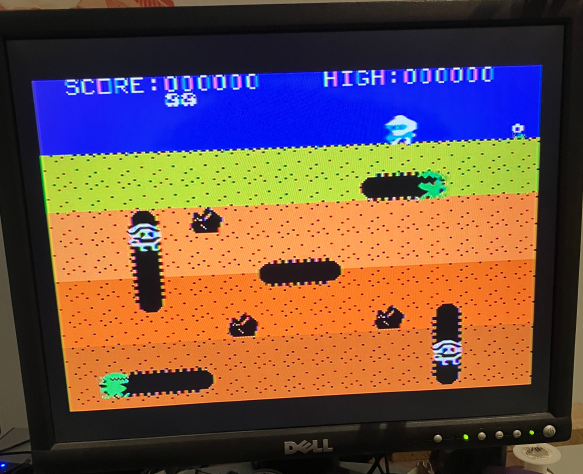
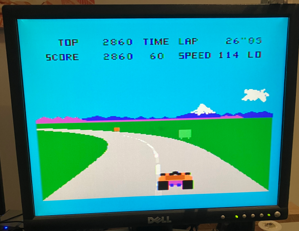
A lot of stuff does work. Some obligatory screenshots below. For all the disk based ones that are ‘XB Autoload’ I used ‘Extended Basic 2.5’
Source
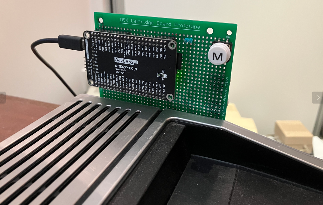
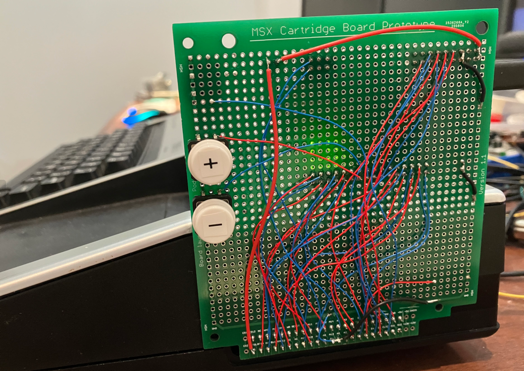
The source is on github in https://github.com/kernelcrash/ti994a-rom-grom-ram-and-floppy-emulator. There’s more detail in the README.md re how to wire it up etc. The photo below looks complicated, but I have my logic analyser and openocd adapter hooked up. You only really need the stm32f407 board, an edge connector and some wires to connect them. On the breadboard, I have the 3 buttons; NEXT, PREV and MENU as well as the 3.3K resistor. Most of the time I just use the MENU button. The other two buttons aren’t that necessary.
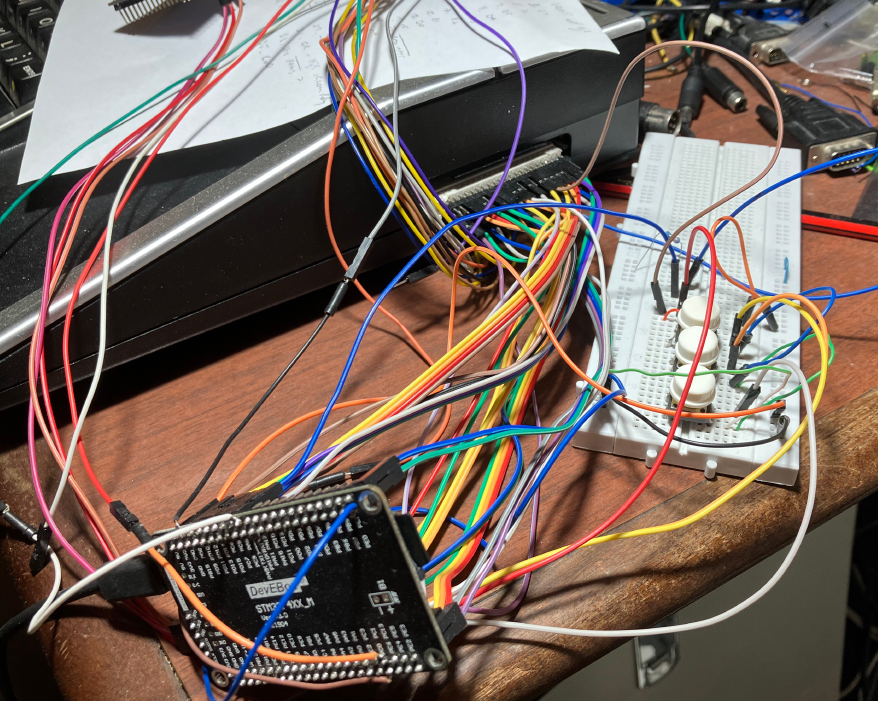
UPDATE. I finally transferred it to some protoboard. These MSX protoboards keep on coming in very handy.