So this is one of my experiments in using AI to fast track some projects (for reference I mostly used Claude Sonnet 5). My basic goal was
- Create a Z80 based computer on a breadboard that doesn’t use many chips and can run the CP/M version of Zork 1.
I’d already tried a minimal Z80 computer where I used the Z80 itself to generate 512×200 two colour composite video. That had the Z80 running at 6MHz, but generating the display as well in horizontal line interrupts, which meant that most of the actual ‘non video’ normal CPU execution time was during the blank part of the screen. I was doing PAL timing, so that meant with 312 lines, I had 112 lines out of 312 that were ‘free’ execution. Unsurprisingly, the real throughput of my 6MHz Z80 was closer to 2MHz. I thought 2MHz was too slow, so I wanted to try something else.
I had a few Atmega1284p chips. They are a 40 pin AVR chip with plenty of internal flash, 16KB of internal RAM, various timers and counters and SPI etc and can run up to 20MHz and they are a 5V chip too. I thought I could use it as a sort of video address generator, and to keep things simple it would simply BUSRQ the Z80 during the active part of each horizontal scanline so that they could share the same physical SRAM. I opted to clock the 1284p at 16MHz. That meant I could do a 640×200 display in two colours. That also meant I could divide-by-two and run the Z80 at 8MHz. Because the BUSRQ’s are roughly 40us out of 64us each scanline, the CPU would get a bit more time per scanline than my earlier design (about 22us) and the overall throughput would be higher. It did work out better, and the rough throughput is over 4MHz which is fine.
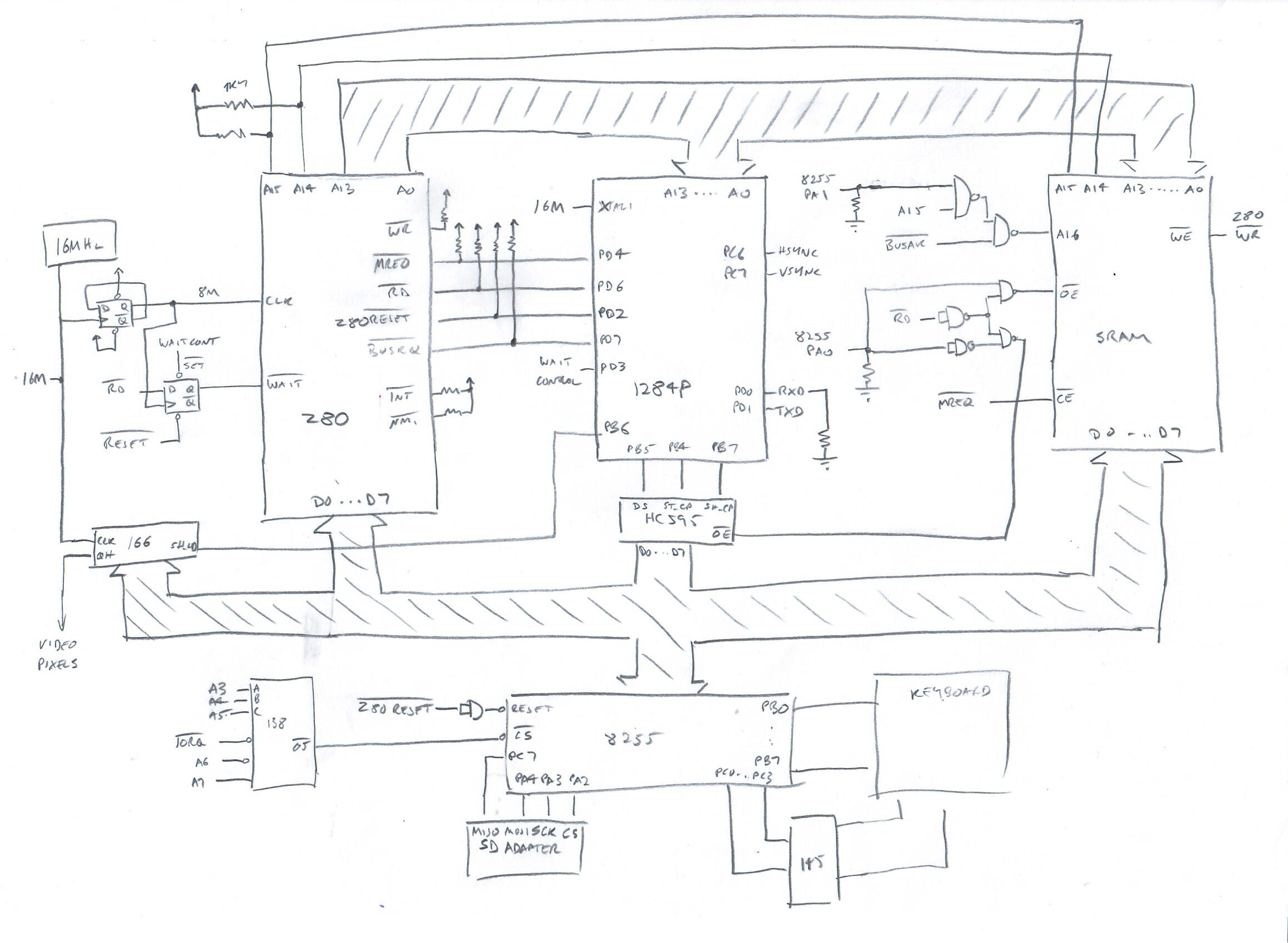
Here’s the rough schematic
Here’s some better close up shots including the circuit for the composite out
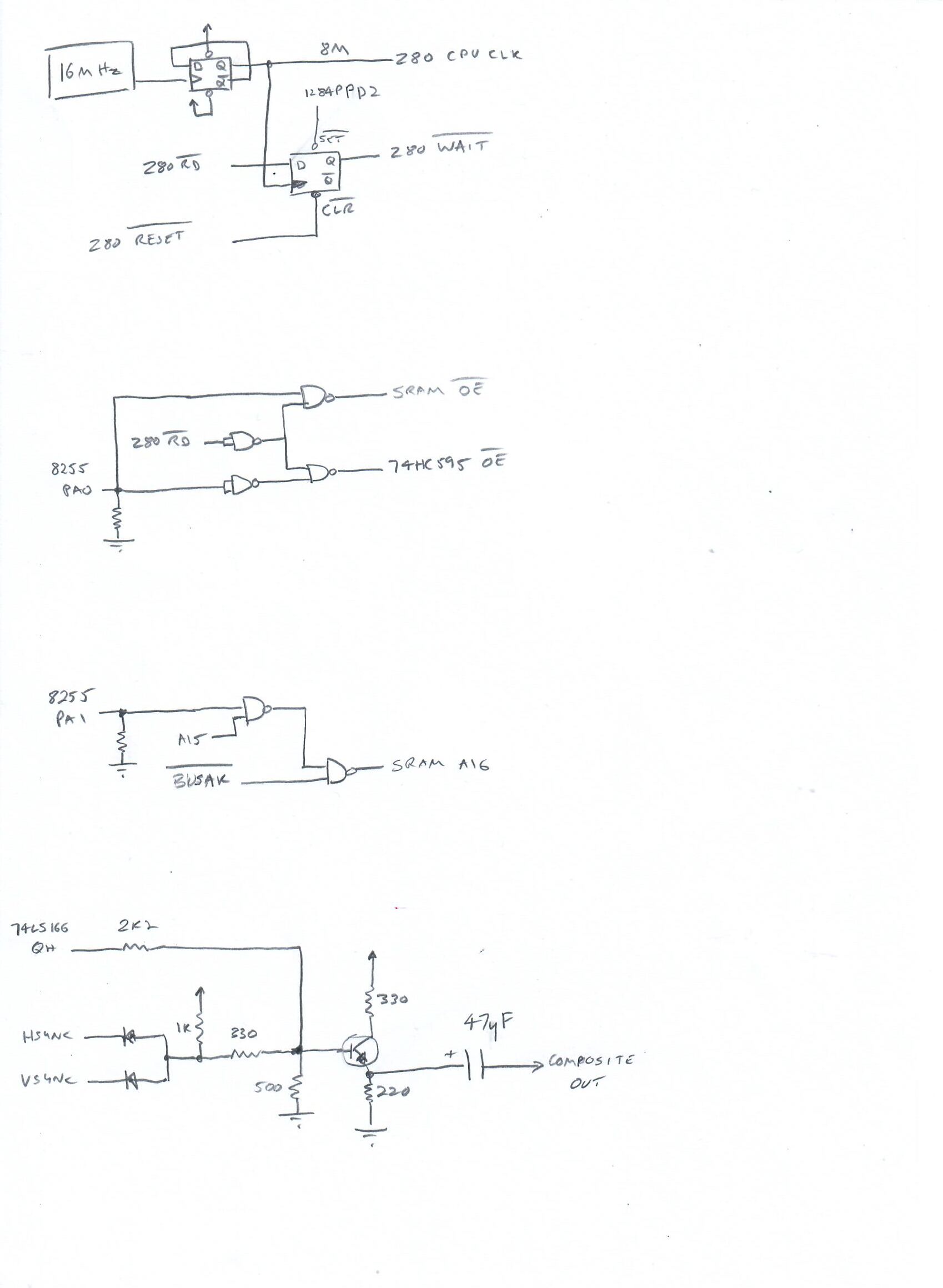
The rough way it works is this
- The 1284p acts as a service processor, but its really the master
- On startup the 1284p holds the Z80 in reset.
- The 8255 is reset such that all its ports are inputs. PA0 and PA1 both have pull downs on them so that means the nand gates to the left of the SRAM behave in a certain way.
- So after reset, when there is a _RD, the nand gates allow the _OE on the 74HC595 to be activated. and the _OE of the SRAM is permanently high.
- The 1284p has an embedded 8KB boot ROM for the Z80. When it releases _RESET on the Z80, the 1284p acts as a ROM emulator. It see’s _MREQ and _RD and the bottom 14 bits of the address bus , so when the Z80 first does its fetch from 0x000 after reset the 1284p will see it.
- There is a D flip flop on the left side that sends _WAIT low after a _RD, and the _SET pin of the flip flop is controlled by PD3 of the 1284p which is ‘wait control’ or ‘wait release’. So the Z80 instantly starts waiting after a memory access. The 1284p then serially pumps the required byte for the ROM emulation into the 74hc595. When its done that , it pauses a bit then sends a pulse to PD3 which releases _WAIT and the Z80 progresses to the next byte it wants to get.
- So the Z80 can run a boot loader type program using this ‘slow’ ROM access. Its something like 3.6us for _MREQ low, so its not a snails pace. The goal of this bootloader is to copy bytes from ROM into the SRAM. The SRAM is wired up to take up the entire 64K address space, but as noted we cannot read from it at this stage since the SRAM _OE is forced high. However, we can write to it, so its a simple case of reading bytes from the emulated ROM and then writing them to the same address.
- Now the SRAM is a 128KB part, and you can see logic that drives A16 to flip between the two 64K parts. We don’t actually use all the 2nd 64K. We only use the top 32K of it. PA1 from the 8255 is effectively a bank control pin, but it only works when A15 is high. There’s also a special case when _BUSAK is low, but we’ll talk about that later.
- So the bootloader busily copies bytes from the emulated ROM into SRAM and at some point we want to stop reading from the ROM, so the 8255 is reconfigured with Port A as outputs and PA0 is finally driven high. This requires that the next instruction to be executed is already in SRAM.
- That still leaves us with slow access, as the flip flop driving _WAIT low is still doing that for the SRAM. To finally end this slow access, we access a magic address 0x3fff. Once the 1284p sees this access it permanently drives PD3 low which forces _WAIT high. This access to the magic address is also the trigger to start video address generation. It also means ROM emulation permanently stops.
- So the 1284p is going to start generating HSYNC and VSYNC signals. And part way into a scanline it sends _BUSRQ low which halts the Z80. It pauses a small amount of time as _BUSRQ is not instant, and the 1284p does not monitor _BUSAK. But once the Z80 has been halted, its address, data and control bus lines are tristated. This is why you have pullups on _MREQ, _RD etc. The 1284p now drives those and starts outputting video addresses on A0 to A13. I only chose to have 14 address pins due to an earlier design not having any free GPIO pins. But our 640×200 two colour screen takes up 16000 bytes so we only need 14 address pins. The A14 and A15 pins have pullups so when the 1284p is driving the bus its effectively addressing 0xC000 and up. And because of the nand gates driving A16 of the SRAM its actually accessing 0xC000 in the 2nd 64K of the SRAM. This whole idea is so that CP/M can see a large program area and the screen is off in another bank.
- The 1284p bumps its video address up once every 500ns. We have a 16MHz pixel clock and the 74LS166 shift register is there to grab the data coming out of the SRAM (as the 1284P will be driving _MREQ and _RD). We use some counter/timer stuff to trigger the SH_LD pulse of the 74LS166 to latch the next screen byte at the right moment.
- The pixels are shifted out and there is a simple NPN driver (I used a BC547) to generate the composite signal.
- The 8255 has a microsd card module hooked up to it (the ones that do the level conversion for you). We have a bitbang driver that can read and write to the SD card.
- The 8255 also has a keyboard matrix hooked up to it. I just used my MSX based keyboard from my Omega MSX2 computer . It has a 74LS145 on it, so the keyboard rows are fed by the 8255 port B and the columns by the 74LS145 using 4 pins from port C.
- And yes I am aware that when the 1284p is in rom emulation mode that a read from an IO device would clash since the _OE on the 74hc595 has no gating for _MREQ. This was a design compromise to keep things simple. It just means that during the initial boot loader run where it copies data to SRAM, that its not allowed to read an IO device.
That’s effectively it. Once the bootloader is running from SRAM, there are additional stages that are pulled in from the SD card so a lot of the code is on SD.
This is where AI came in very handy;
- it wrote me a SD card bit bang driver
- it wrote me a keyboard matrix scanner
- it ported CP/M 2.2 to this platform.
In order to keep things simple the system doesnt have a simple FAT32 driver to access the SD card. Instead you need to dd to the 1st and 2nd MBR partitions of the SD card. The 1st partition is effectively drive A: and the second is drive B:, but to make things more useful, drive B: is a 50MB hard drive. There are scripts provided to take files from your PC, and generate the partition images.
You’ll see on the circuit that the PD0 RXD usart pin is tied low. That’s basically a signal to the 1284p to use its own internal flashed copy of the boot rom and make it available and take the Z80 out of reset immediately. If I have a usb-serial device plugged in there and actively connected to another computer, that pin will end up high and the 1284p holds the z80 in reset and has a small monitor terminal mode that it boots in to. In this mode, you can xmodem the boot ROM to the 1284p and then tell it to start (‘s’) command. So that’s great during development.
An earlier design I had used a 74LS373 where the 74HC595 is. That used more GPIO pins and was only marginally faster. I thought I’d try switching to the 74HC595 to free up some GPIO pins. There are still a number of free pins.
The design takes up around 2 and a half 830/840 point breadboards. The photo shows 4 of these breadboards hooked together and really the computer takes up all of the left two and maybe 2/3’s of the 3rd one (I have the SD card adapter on the right most one, but it could move to the the breadboard to the left of it).
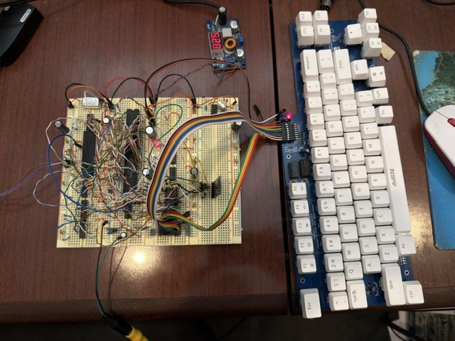
So it does CP/M
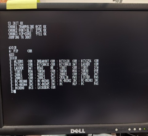
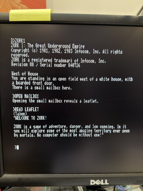
So yes it can run Zork 1.
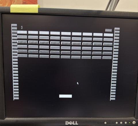
I also got AI to write a simple breakout game for the system:
And for some gargantuan project that blows my Claude 5 hour and weekly limits constantly, I decided to see if Elite could be ported to it. Originally I started with a disk image for Elite for Amstrad CPC, thinking the 16000 byte screen buffer might simplify things (ie. Both the CPC and this system use 16000 bytes. And yes I am aware that the address structure is different and also that the CPC did not use 640×200 mode). It didn’t help. So then I thought I would try getting it to read the well commented BBC Micro 6502 code for Elite and use that as the basis to translate to Z80 code. And claude made a good start on this … but after a week or two of slow progress I decided to forget the port and focus on spending my tokens on other projects.
Source is at https://github.com/kernelcrash/breadboard-z80-1284p-cpm