A few months back I came across an ebay ad for a circuit board for a Galaksija. I had never heard of it before. The original Galaksija came out in 1983 in Yugoslavia. The Galaksija wikipedia page has a lot more info and the spetsialist-mx.ru site has a big section on it (in Russian). That site also has a lot of info on various clones and enhancements. I ended up ordering the circuit board which turned out to be a remake of the ‘Galaksija Plus Clone by PVV (PCB by Fifan)’ . It’s mentioned on the spetsialist-mx.ru page on Galaksija Plus machines. It had the circuit diagram plus dumps for the two onboard EPROMs as well as some files to shove into an SD card (as this particular ‘Plus’ had an SD card socket onboard).
The way the Galaksija produces video is very interesting. I am big fan of the older computers that used their own CPU to generate video. In my misspent childhood I was very proud of understanding how the ZX-80 produced video using its CPU. There is some more technical information about the Galaksija at revspace.nl , including a link to a (translated) technical document written by Tomaž ŠOLC as part of a University Thesis on how the Galaksija worked. It’s a great read.
To me one of the really cool bits of the Galaksija is how they used the Z80’s I and R registers as a sort of video address counter. I’ve played around with Z80’s for a few decades and you always knew that in the 2nd half of an instruction fetch (M1) cycle that _MREQ went low again and the R register was shoved on the lower address lines as a way to refresh dynamic RAM chips. The R register would get incremented between M1 cycles and so long as _RAS went low during these ‘refresh cycles’ you could refresh dynamic RAMs without lots of additional circuitry. But it was only a 7 bit counter, so 4116’s was about as big a DRAM as it would work with without additional circuitry (I think 4116s may have only just come out or were in the future when the Z80 came out in 1976).
Of course the Galaksija does not use Dynamic RAM at all. The original just used one or more 6116 static RAMs. What I didn’t realise with respect to the Z80 refresh cycles is that the I register is on the upper part of the address bus when R is on the lower 7 bits. So with I on A15-A8 and R on A6-A0, you are only missing A7 in terms of having a full 16 bit video address counter. In the case of the Galaksija, they solve that with a couple of gates and a latch. ie. you can set A7 to 0 or 1 as needed for a refresh cycle.
With only a couple of KB of static RAM, the Galaksija was not going to do bitmapped graphics easily, so it has a 2nd EPROM as a character ROM. So during the refresh cycle RAM is read. The byte read from RAM ends up being some of the address lines to the 2nd EPROM. Then a latch provides a few more address lines, and bingo you have character graphics.
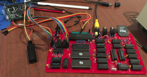
So here’s an early shot of the board mostly completed. I had a fair bit of trouble getting video output 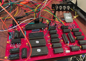 to initially work. In hindsight, some stuff in the Galaksija design is a little ‘marginal’, and really wants ‘chips from 80s’ . So while the Z80 does a lot of the address generation etc, a bunch of counters and one shots are used to generate sync pulses. The basic deal is:
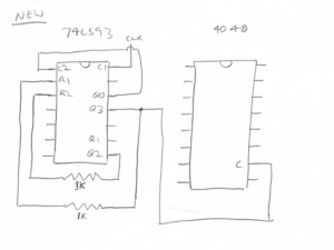
6.144MHz crystal clock. Divide that by 12 using a 74LS93 and you get 512KHz. Then a 4040 is used. The ‘divide by 32’ gets you 16KHz, and the ‘divide by 1024’ gets you 500Hz. Shove the 500Hz into a 4017 to ‘divide by 10’ and you get 50Hz. The 16KHz generates your horizontal sync (which is ‘close enough’ to 15625Hz or 15750Hz), and the 50Hz generates your vertical sync.
So I had a lot of trouble with the ‘divide by 12’ part, or possibly a problem with the combination of the 74LS93 and the 4040. I tried different 74LS93’s and I had some 74HC4040’s and an older 4040. Generally I would see the 74LS93 dividing by 8 instead of 12. To me the 74LS93 is configured in a strange way to divide by 12 by utilising the two (active HIGH) reset lines on the 74LS93. In the photo above I ended up working around it by tying one reset high and then using the Q2 and Q3 outputs of the 74LS93 into an AND gate to drive the remaining reset. That worked, and I did indeed get a picture;
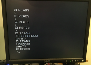
Yep, I got to write non-sensical things by shorting some of the keyboard wires together because I have not got a keyboard for it.
However, it was still bugging me having that AND gate hanging off the back of the circuit board. I thought it is most likely to do with some small glitches when the 74LS93 counter is ticking over, so I tried playing with some resistors or caps to induce a sort of filter on the reset lines.
I came up with this that seems to work OK (for me). I just cut some traces and put 1K resistors in between the counter outputs and the reset inputs. And now it divides by 12 OK. I will note that I am using a 74HC4040 for the next counter stage.
So that gave me video output. What about the keyboard?. I could opt to make one up. However I had made a sort of keyboard emulator for an Oric Atmos mainboard some time back. That used s PS2 keyboard plugged into an Arduino Uno. You hit a key on the PS2 keyboard, then the Arduino Uno looked for the row/column scan stuff coming from the Oric and effectively ‘pressed a key’ at the right moment. That worked OK-ish. It never worked 100% which I assumed was related to the speed of the Uno.
So given I spend a lot of time looking at stm32f4 boards, I had a go at making a keyboard emulator using one of those boards. And that works pretty well. Response time is a lot better than the Uno as well. More details are at https://github.com/kernelcrash/keyboard-matrix-emulator .
Here it is connected up:
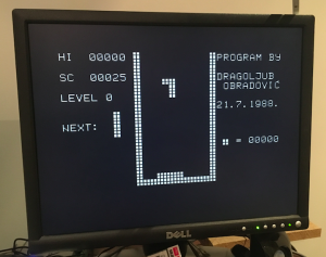
And finally I can play Tetris