It’s summer here, and I was trying to think up interesting projects I could do with my son over the xmas period, and one idea was to put together a Dick Smith Funvision on a breadboard. Before you get too excited, this project was more about the process of making a computer, rather than trying to make a perfect replica of an 80s home computer.
I had a Funvision when I was younger, but gave it away to a good home a few years ago. It is in fact the VTech Creativision in one of its many rebranded connotations. It came out around 1983/1984. Google seems to completely fail when trying to find an image of a Funvision so I fished through some old photos I had of mine before I gave it away (UPDATE; I did eventually google some Funvision pics here)
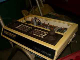
It’s a bit dirty (was stuck in a shed for many years) and is missing the top ‘fake wood’ panel. It looks much the same as the Hanimex Rameses. My older brother had a Funvision too, but his is incomplete as well.
The goal
Anyway, here was my summer ‘project’ goals;
- Build a computer on a breadboard
- Have it do something useful when we’ve finished building the hardware.
Part 1 meant quite a few things; I had to have all the parts for a Funvision (or most of them). They had to be parts that would go into a breadboard (ie. DIP chips). The circuit design couldn’t be too outrageously fast or complicated as breadboarding doesn’t really support all the types of computers you can make on a circuit board. I did have most of the parts. The basic hardware recipe for the Funvision is pretty small;
- 6502A CPU @ 2MHZ
- 1K of RAM (in two 2114s)
- 2K boot ROM plus additional game ROMS in cartridges
- 74LS04, 74LS32 and 74LS139 for clock and address/rw decoding
- 9929 VDP (since Australia has/had PAL TV)
- 16K of Dynamic RAM dedicated to the VDP
- 6821 PIA
- 76489 sound generator
- TBA520 colour chip
That was pretty much it. It is quite similar to a Colecovision (same Video and Sound chip, but different CPU). In 2015, it is still quite easy to obtain all these chips in DIP form. Regardless, I have a ‘big box of chips’ and had pretty much everything (or close approximations) except for the TBA520. I thought it was unlikely I would get good colour output anyway, so the goal was black and white composite output.
Part 2 (‘do something useful’) means that once I have the thing wired together I have some boot ROM to boot and usable programs for it. The alternative is to make a bespoke computer that has no software for it (and hence I would have to write some kind of machine code monitor and loader just to be able to do anything). There have been a few emulators written for the Creativision over the years so there are ROM dumps available so I should be able to get some games going on it.
What about a joystick? The Funvision had slightly strange (for the time) joystick/half-keyboard controllers. Each joystick also had 24 membrane keys on it that formed one half of a QWERTY keyboard when inserted into the main unit. These had a really strange key matrix … so initially I decided to borrow my brothers’ Funvision controllers. The Funvision predates the era of annoyingly uniquely manufactured plugs and sockets, so the controller connectors are simple 0.1″ spacing pin headers.
Slight hardware changes
Rather than use exactly the same set of chips, I thought I’d make a few seemingly minor changes
- Use a 65C02 rather than a 6502A
- Use a 32K cache SRAM (in my case UM61256AK-15 from a very old PC motherboard)
- Use a flash rom (29F040)
I actually had a 6502A, but I recently bought a WDC 65C02 and thought things like the ‘Bus Enable’ might come in handy later on. I did know at the outset that a 65C02 is not 100% compatible with the 6502 … but thought given the small number of games available for the Funvision, I was unlikely to hit any compatibility problems
Fitting two 2114’s for 1K of ram seemed a bit silly. I have heaps of old 2K (6116) SRAMs and was going to use one of those, but I also have a lot of 32K cache SRAMs off old PC motherboards (we’re talking 386/486 and early pentium era) and I thought I might want to extend the basic 65C02 design later. But the idea was to tie most of the high address pins low such that it appeared as 1K anyway.
Using a flash ROM was to address a few things. So rather than add in a real cartridge edge connector and connect real Funvision cartridges, I would write the game images to a large flash rom and change the high address lines to alter which cartridge was active. I would have still needed another ROM somewhere for the 2K boot ROM, and I was conscious that I would probably run out of space on my breadboards. If I could combine the boot rom and game images in one, that would be good.
Now, the original Funvision memory map is a bit like this;
- $C000 to $FFFF is the 2K boot ROM repeated 8 times.
- $8000 to $BFFF is the initial 16K page for cartridge ROMS. There is a 2nd 16K page for cartridges at $4000 to $7FFF but not a lot of games used the extra page.
the idea was to split the flash ROM into 32K chunks. The 29F040 is a 512K part, so that’s a lot of 32K chunks. In each 32K chunk , the lower 16K would be a cartridge mapped into the $8000 to $BFFF region and the upper 16K would be the boot rom repeated 8 times. I would then change the address decoding such that whenever the 65C02 top 32K was selected (A15 high) it would select a 32K chunk of the flash rom (I would just tie the ROMs A15 to A18 to combinations of GND and +5V to select different images).
I just did this in linux to build up these 32K chunks (for example with the 4K Sonic Invaders image)
  cat FUNBOOT.ROM FUNBOOT.ROM FUNBOOT.ROM FUNBOOT.ROM \
    FUNBOOT.ROM FUNBOOT.ROM FUNBOOT.ROM FUNBOOT.ROM >16KFUNBOOT.ROM
  cat SONICINV.ROM SONICINV.ROM \
   SONICINV.ROM SONICINV.ROM >16KSONICINV.ROM

  cat 16KSONICINV.ROM 16KFUNBOOT.ROM >32KCART1.ROM
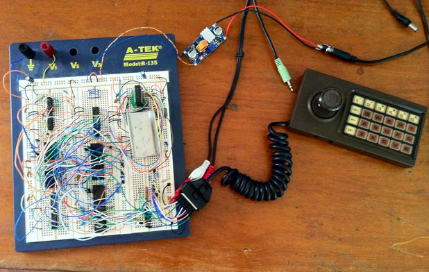
Basically just repeat that sort of thing for other games. For an 8K game you only need to repeat the image twice to fill up the 16K. In each case you need to combine a 16K cartridge chunk with the 16KFUNBOOT.ROM. Once you have a series of 32K chunks you then need a means of programming a flash ROM. For me, I’ve recently invested in a willem programmer which conveniently programs these types of flash rom. I’ll note at this point that not everyone has a Flash ROM programmer and there are many alternate ways of getting something bootable into your system. I ended up (later) using an alternate method using a battery backed SRAM. You can just hook up an Arduino Uno and a 4040 counter to one of these, program it, then transfer it to the target system.
First Steps
Ignore the bit about 32K chunks in the flash ROM for a moment. Sure this hardware design is relatively simple, but there are still a lot of wires … and a lot of opportunities to get things wrong. This is actually one of my reasons for doing this whole project; it teaches you to be very careful because trying to find a mistake in a maze of wires is somewhat difficult. No one can help you 😉 One way of mitigating some of the risk is to build the computer in stages. Less wires equals less chance of failure.
So first step for me is getting a computer to boot and blink an LED. To do this we’ll need to wire up the following;
- 74LS04 and a crystal to generate a CPU clock
- 65C02
- 74LS139 to do some address decoding
- 29F040
- 74LS374 with one of its inputs tied to the CPU D0 and the corresponding output going to a 270R resistor and then an LED to GND.
You need a 5V PSU as well. I’ve bought a few LM2596 based PSU’s off ebay recently. They are cheap tiny switchmode supplies. You feed in 12V DC or similar, adjust the trimmer to get around 5V and then dont touch it again. Make sure you get it producing 5V before you attach any chips to it. I adjusted mine to around 5.2V since I knew I would probably have voltage droop across my breadboards.
So this ‘first step’ is close to parts of the Funvision; 74LS04, 6502, 74LS139 and a rom, so you can see how they did it on the real Funvision and do it the same. the Creativision schematics are on the Madrigal site, but I also found them in my old paper notebooks from 30 something years ago.
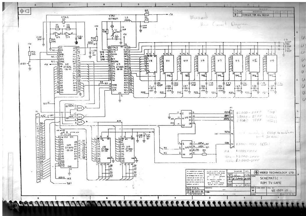
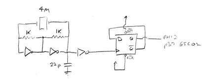 The Funvision crystal oscillator is two inverters and a 2MHz crystal and some caps and resistors. I didn’t have a 2MHz crystal handy, so used a 4MHz crystal instead and fed it into one half of a 74LS74 flip flop acting as a divide-by-two stage. The 2MHz output of that goes to pin 37 of the 65C02.
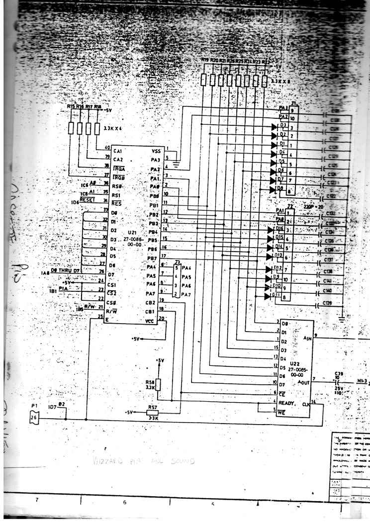
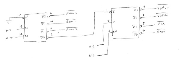 Address decoding in the Funvision is done mainly with the 74LS139. One half divides the 64K of memory into four 16K pages, and the second half of the 139 decodes the bottom 16K into 4K pages (for RAM, PIA and separate chip selects for read and write into the VDP).
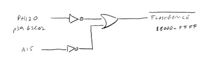
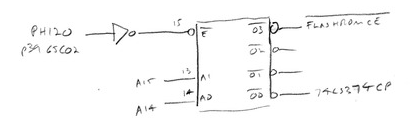 For my ‘blink the LED’ test I only really needed the address decoding done by the first half; top 16K (ROM0*) will be my flash rom, and one of the other three will be to the clock input of the 74LS374. One thing I changed at this stage was how the Funvision has the Enable* input tied to GND. This makes sense for the original Funvision as ROMS were a lot slower back in the day, and basically the ROMs chip enable goes low as soon as the address bus lines stabilise which gives it long enough to get data on the bus. Think of it this way; if your ROM has an access time of 250ns, and the CPU cycle time is 500ns (ie. 2MHz clock) then you need your chip enable to go low before the middle of your 500ns cycle. But my flash ROM was somewhat faster, so I used an inverter out of the 74LS04, inverted PHI2O (p39 of the 65C02) and ran that into the Enable* on the relevant side of the 74LS139. So with that I wired up the rom and the 74LS374 in a memory map like so
- $0000 to $3FFF – 74LS374 clock input
- $C000 to $FFFF – flash ROM CE*
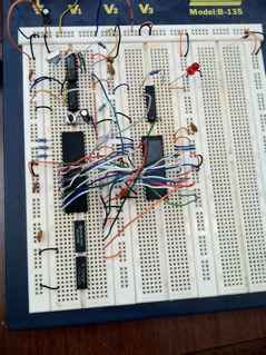
So the photo to the left shows the 74LS04 and crystal related circuitry in the top left. Below that the 74LS74, a reset button, then the 65C02. There’s a few extra pullups on a 65C02 compared to a 6502. One thing I will note is that I had never used a 65C02 before this project and didn’t realise that there are at least two different types of 65C02. Mine is a WDC 65C02 which has a different pinout to a Rockwell 65C02. Below the 65C02 are the 74LS139 and 74LS32. Then the next column has the 74LS374 and associated LED and the 29F040 flash ROM below it. One discrepancy in the photo is that at the time of the photo, the 74LS374 was wired to the $4000 to $7FFF chip select of the 74LS139, rather than the $0000 to $3FFF output mentioned in this article.
I created a tiny blink test program using atasm (output in raw) and had a 16K binary file that I could use with my Willem to program the bottom 16K of the flash ROM.
*=$C000
; this is just so there is some starting point
        LDA #$00
*=$FF00
; LED is wired to bit 0 of ls374
ls374 = $0000

start
        LDA #$01
update  STA ls374
delay   LDY #$FF    ; load Y with $FF
loop1   LDX #$FF    ; load X with $FF
loop2   DEX         ; X = X - 1
        BNE loop2   ; if X not zero goto loop2
        DEY         ; Y = Y - 1
        BNE loop1   ; if Y not zero goto loop1
        TAX
        INX
        TXA
        JMP update

*=$FFFA
nmi     .word   start
reset   .word   start
irq     .word   start
So with programmed flash ROM in place and the flash ROM’s A14 to A18 tied low, I tried powering up. I don’t think it worked. A handy gadget I have now is a 16 channel logic analyser. I never had one back in the 80s. It is handy, but I dont think its essential for this sort of stuff, but I hooked it up to to the PHI2 clock and the databus to see if I could see anything. I think I had a problem with my crystal oscillator starting. There seem to be a heap of different ways of doing crystal oscillators with inverters. I had put a typical low pF caps to GND from both sides of the crystal, but for whatever reasons the clock wasn’t ticking over. Removing one of the caps seemed to guarantee it starting up. 😉
And then it seemed to work. I got a blinking LED.
Building the rest of the Funvision
So with confirmation that I had a basic 2MHz 65C02 setup working, I decided I would add in the rest of the chips. I reverted the address decoding so that it exactly matched the Funvision. There is also a 74LS32 in the Funvision design that gates the VDPR*, VDPW* and SRAM WR* to the PHI1O output. I added that as per the Funvision circuit diagram.
 Next I rewired the flash ROM. As noted earlier, I was going to make it appear as a 32K ROM from $8000 to $FFFF, so I used another inverter and the unused OR gate in the 74LS32 to generate a chip enable for my 32K images. A15 to A18 of the flash ROM were all tied LOW, but I used jumper wires that were a bit longer so I could easily change between +5 and GND and hence I could select other images in the flash ROM.
Then I wired up the 32K SRAM. So this is wired just like the 2114’s in the original design except that A10 to A14 are tied LOW. I also tied OE* LOW.
Next is the VDP and its DRAM. So the original Funvision had eight 4116 DRAMs. 4116’s are a pain to use as they require a +5V and +12V and -5V power supplies. A simplification is to use eight 4164’s. These are 64Kbit DRAMs so you are effectively wasting 48K, but they only require a single +5V supply. DRAMs in general (at least these older ones) are a bit problematic when it comes to circuit board design. My experiences in my youth are that you can wire up DRAMs on a protoboard like a vero board but they may not work 100% reliably. Back then I ended up making my own PCBs with just a 9929 and the eight DRAMs on it. So how to do this on a breadboard? One design I had done in the past to increase the chances of the DRAMs working well was to piggyback all of them. 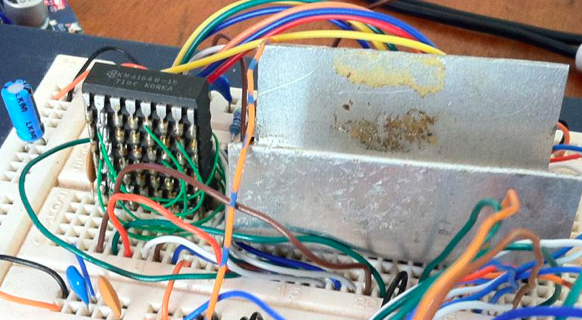 So essentially you solder eight 4164’s on top of each other but with pin 2 and 14 of each chip bent out a bit so they don’t touch the pin below them. In the Funvision design all the DRAM pins are soldered effectively in parallel except for pins 2 and 14. Each of the independent pin 2’s are then soldered to one of the DRAM address pins (these are all the green wirewrap wires in the photo to the left) as the VDP puts its ‘write data’ onto the multiplexed address bus. My wiring detail for the pin 2’s working from the top chip to the bottom is
- Top 4164: pin 2 to pin 5 (A0)
- pin 2 to pin 7 (A1)
- pin 2 to pin 6 (A2)
- pin 2 to pin 12 (A3)
- pin 2 to pin 11 (A4)
- pin 2 to pin 10 (A5)
- pin 2 to pin 13 (A6)
- Bottom 4164. pin 2 is not wired to an address line. Instead you connect it on the breadboard to pin 10 (DA0) of the 9929.
And the pin 14’s are independently wired to all the RDx pins of the 9929 (all the multi coloured wires in the photo to the right).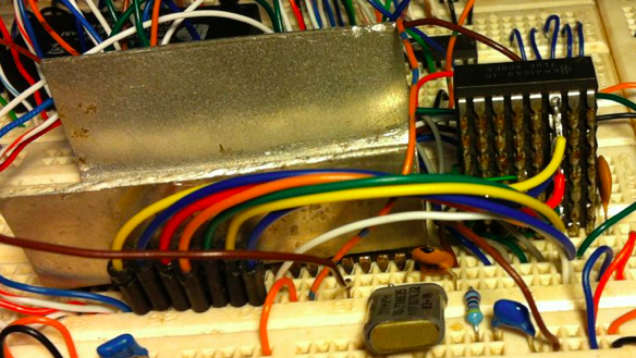 For reference, the big chunk of aluminium is the heatsink I made and glued to the top of a 9929. The 9929 gets quite hot and all designs I’ve seem put a heatsink on them. You just glue a chunk of metal onto it. It doesn’t need to be as big as the one I have.
Wiring up the 9929 is straightforward and is as per the Funvision circuit diagram. With regard to the 10.738635 MHz crystal you can just put in some low pF caps to GND (I used some 22pF caps) on each side of the crystal rather than the more complicated setup on the Funvision circuit diagram. In 2015 the 10.738635 MHz crystals are a bit hard to find. However, I’ve seen them listed at mouser, digikey and even some aliexpress sellers. Also, I’ve actually been looking at getting a 9958 recently and see that the 21.47727MHz crystals (ie. twice 10.738635) are a bit easier to find. You could in theory then divide by two to get 10.738635.
I should note here that the 9929 is the PAL version of the 9918. My Funvision was a PAL model (since it was bought in Australia). There were NTSC versions of the Creativision sold in other parts of the world which used a 9918 instead. I happened to have a couple of 9929’s when I started this project, but I am tempted to get a 9918 and swap that in instead. The key advantage of the 9918 is that it puts out full NTSC colour. In Australia in the 1980s, a 9918 would have been quite useless since no one had an NTSC TV. But in 2015, modern LCD TV’s tend to handle PAL or NTSC reasonably well … and so it’s probably a simpler option for getting colour to just use a 9918 instead (of course the games will all run slightly faster, since the vertical blank interrupt will be 60Hz instead of 50Hz).
So the wiring of the 4164’s is much the same as the 4116’s in the Funvision circuit diagram. The main differences are pin 1 is not connected and pin 9 is tied HIGH with a resistor (I just used a 4k7).
One huge disadvantage of the vertical stack of 4164’s is how on earth to add in eight decoupling caps around them. You could try to solder them to the chips themselves, but I have just put several around the +5 and GND lines near the chips. This isn’t great, but works well enough.
Another thing to note about most 9929/9918 designs is that they had a huge ground plane around the DRAMs. On a breadboard this is really hard … so I just don’t have a big ground plane. While doing research for this project I came across the Vulcan 74 project which is far more ambitious and cool than what I’m doing. Interestingly one of the photos in that thread show the breadboards stuck onto an oven cookie tray to provide a better ground plane. I am curious to try that to see how well it works.
The only other thing left with the VDP circuitry is some kind of transistor amplifier to generate a useable composite output. I used this;
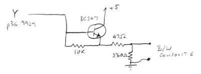
Next up is the 6821 PIA and 76489. I wired these up as per the Funvision circuit diagram. The p25 E input of the 6821 comes directory from the PHI2O of the 65C02. And for the audio output of the 76489, the -ve side of the 10uF electrolytic can be wired straight to an RCA audio lead to go to your TV.
I initially only wired up the left hand controller as you need at least this one to do one player games. I just wired up the diodes (1n914’s or 1n4148’s) and the pullup resistors and left the 220pF caps out. The left hand controller is the one wired to PA0 and PA1 of the 6821. The pinout of the controller ports (ie. looking at the Funvision motherboard from the front is like this;
Left hand controller
PB5 PB6 PB7 PB4 PB3 PB2 PB1 PB0 PA0 PA1
ie. it’s the opposite way around if you are holding an actual controller plug in front of you looking at the 0.1″ spaced holes. So the left most hole is for PA1.
The right hand controller port is
PA2 PA3 PB7 PB6 PB5 PB4 PB3 PB0 PB1 PB2
And again, if you are looking at the plug attached to the controller with the 0.1″ spaced holes directly in front of you then PB2 is the left most hole.
Per the pinouts above, all the PBx pins are obviously after they pass through their related diodes. ie. PB0 is actually the cathode of D16 for the left hand controller.
Now, most people will not have a Funvision controller handy. They are kinda strange too. Most keyboard matrix’s are a simple row and column affair. Basically all the keys are arranged in a grid. You have some IO port output a LOW on each row in turn, and then some input port reads all the columns looking for a single line pulled low which would indicate a key press. The Funvision is not like that. For starters there are only really two row strobes per controller (eg. the left controller can only strobe PA0 or PA1 low). And you always have two lines going low in the column outputs, not one. There is a tech document that comes with the Funnymu Funvision emulator that mentions this behaviour, and if you look at the funnysdl.c source you’ll see that the emulator simulates these ‘two lines go low’ behaviour. eg. if you press ‘q’ then
case SDLK_q: KEYTBL[13]&=0xe7; break;
0xe7 corresponds to both bit 3 and bit 4 going low. And KEYTBL[13] is used when PA1 is strobed low. In theory, if you made your own keyboard matrix you would need to use double pole pushbuttons so that each button can drive two of the PBx columns low. A similar thing happens with the joystick. Each direction drives two lines low, not one. A perhaps easier method (though kind of cheating given the old-school nature of this project) is to use an arduino to simulate the PBx responses. eg wire an old atari joystick and a couple of pushbuttons to an arduino and the arduino will generate the two lines low effect for you. Another way would be to redo the key scanning routine in the boot ROM to use a different type of key matrix. It’s unlikely that games ever tried to use their own key scanning routine since it was so weird.
And here it is. The main changes from the earlier photo are; down the middle are the 32K SRAM , the flash ROM and the 6821, and down the right is the stack of 4164’s, the 9929, the transistor amp (hard to see) and the 76489 down the bottom. Plus I have a real Funvision controller hooked up.
And did it work? No.
What did you expect ? 😉
OK, so there is a lot of wiring, so I did lot of poking around to see if I had miswired anything. Then I hooked up the logic analyser to the databus, the PHI2O and the reset signal. I could see it reading stuff after RESET* but not the reset vector I was expecting (which should be $FF66). More poking around and I noticed that I had not wired up A14 to the flash ROM so it was only ever addressing the lower 16K of the 32K image I had setup. So I fixed that.
And it still didn’t work. I did have some blank output with vertical banding on the screen though which was at least stable … which told me the VDP was doing something and was generating decent horizontal and vertical sync signals. Running the logic analyser again I could see it reading the right reset vector and reading the right code from the boot rom … so it seemed to be working OK. But I still had nothing on screen.
I slept on it. I had a theory that gating a lot of the signals to PHI1O (VDPR*, VDPW* and SRAMWR*) was wrong, and I should be gating them to PHI2O since PHI2O is more closely aligned with the end of the real CPU cycle. I had some vague idea that maybe my 15ns SRAM was too fast or somesuch. I rewired it all using the inversion of PHI2O and I got this;
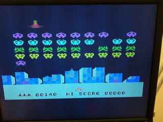
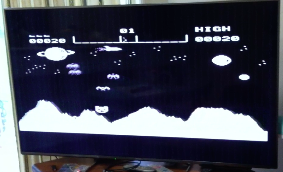
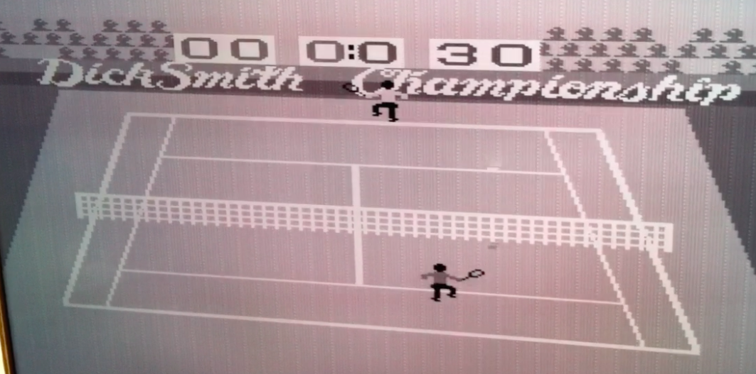
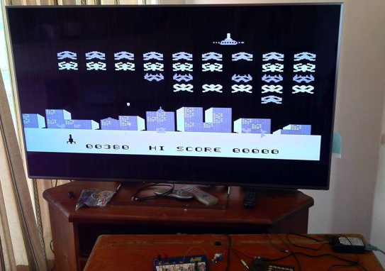 Yes, success. Sonic Invaders in black and white on a 65 inch 4K TV! It’s something I always dreamed about in 1984 ;-). So it all works. The left controller works fine (for reference, you had to press the RESET button on a Funvision, then select a level using the controller fire buttons, and then press ‘6’ or ‘B’ to start the game). And I have full sound.
I tried a few more games that I had imaged to the flash ROM. Astro Pinball worked. So too did Planet Defender. Oddly Crazy Chicken started up, but died as soon as there was a sprite to playfield collision. Maybe that one is related to my use of a 65C02. Police Jump and Mouse Puzzle worked and Tennis also seems to work (but I think I need to wire up the 2nd controller for that one).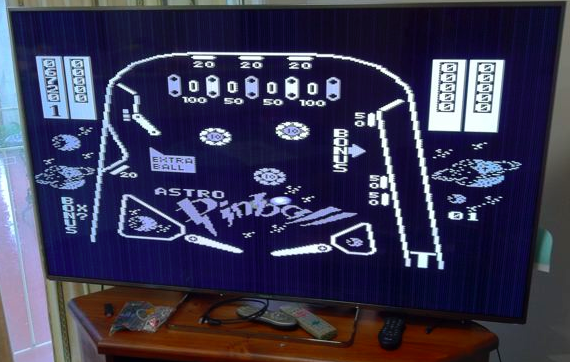
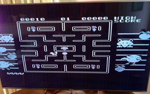
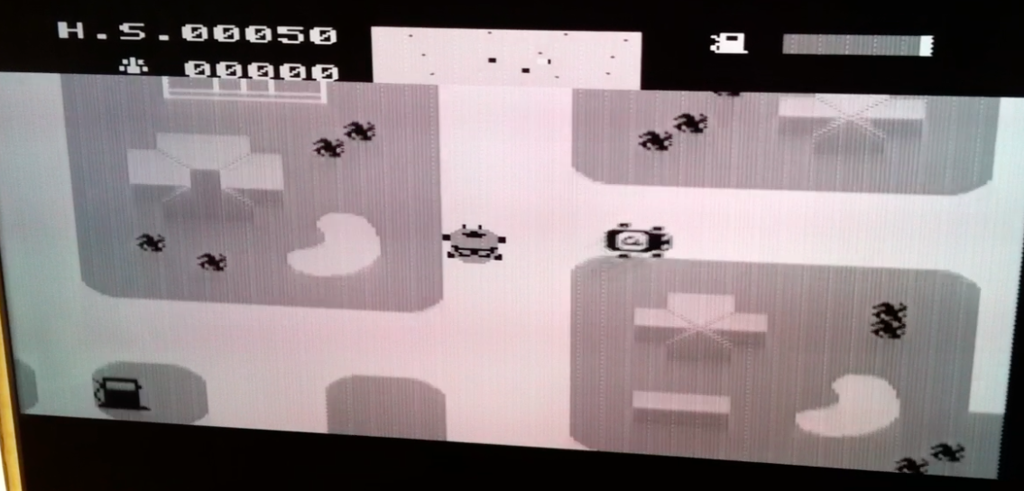
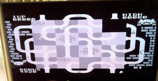
You can see vertical banding in all the photos. Some of that is the typical ‘sampling’ that modern LCD’s do. Other screen issues are probably to do with the lack of a decent ground plane. It is pretty good in general. I was at my parents house on holiday when I got it going and used their 65 inch TV. However, I’ve since tried it on my Dell 2001FP and everything looks a lot nicer when it’s not ‘so big’ and also in 4:3 rather than widescreen.
Interestingly, in the course of writing this up, I thought I would replicate my initial fault with the address decoding and PHI1/PHI2 stuff so that it is wired as per the Funvision (ie. the bit that didn’t seem to work initially) … and hey it actually works wired up per the Funvision circuit diagram! So, now I’m not sure what actually went wrong that first time round. Maybe something else was loose. Who knows.
Colour?
I was pretty happy with getting black and white composite output working OK, but thought I should at least have a minimal attempt at getting colour working. Now I did not have a TBA520 or a LM1889 (as used in the Colecovision) for getting colour composite working. However, the 9929 puts out Y, B-Y and R-Y signals which are kinda sorta maybe the same as modern component video output. If you poke around the forums for Colecovision and various other 9929/9918 based systems (eg MSX) you’ll come across various attempts to hook them up to the component inputs of a modern TV. Attempts vary from basic transistor amps to complex op-amp setups. There often doesn’t seem one ‘this is the way you do it’.
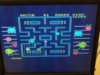
One very simple but not necessarily perfect component mod is mentioned in this NFGGames thread. Basically you need an NPN transistor a 470 ohm pulldown and some kind of series output transistor (see ‘reply 6’ in that thread). I initially used a 100 ohm series output resistor, but later changed them to 150 ohm ones. So I did this to all three 9929 outputs ; Y, R-Y and B-Y. Not sure if Y is meant to be setup differently since it also contains ‘sync’. Anyway, I hooked that up and hooked the outputs up to the component inputs on my Gonbes 8200 and ran the VGA output into my Dell 2001FP and hey I have Colour!. It is seriously ‘blue’ though (which I think would require some more complex circuitry to fix) , and the vertical banding seems worse than before, but it’s pretty cool nonetheless.
UPDATE: I did persist on in trying to get better component video output from the 9929. Also read the note about the quality of breadboard to use at the end of Recreating the Colecovision. My 30 yr old breadboard turns out to be a lot better quality than the really cheap breadboards available today (2016) … and you need a good quality breadboard for this project. Read Comparing breadboards for more info.