A few years back I built a Funvision , then later a Colecovision using a breadboard. These were fun projects and I always thought there were quite a few other 1980s computer designs that were ‘achievable’ within the limitations of breadboards. To me these are good educational projects and you have to plug together seemingly hundreds of wires exactly correctly for the whole thing to work. Fun!
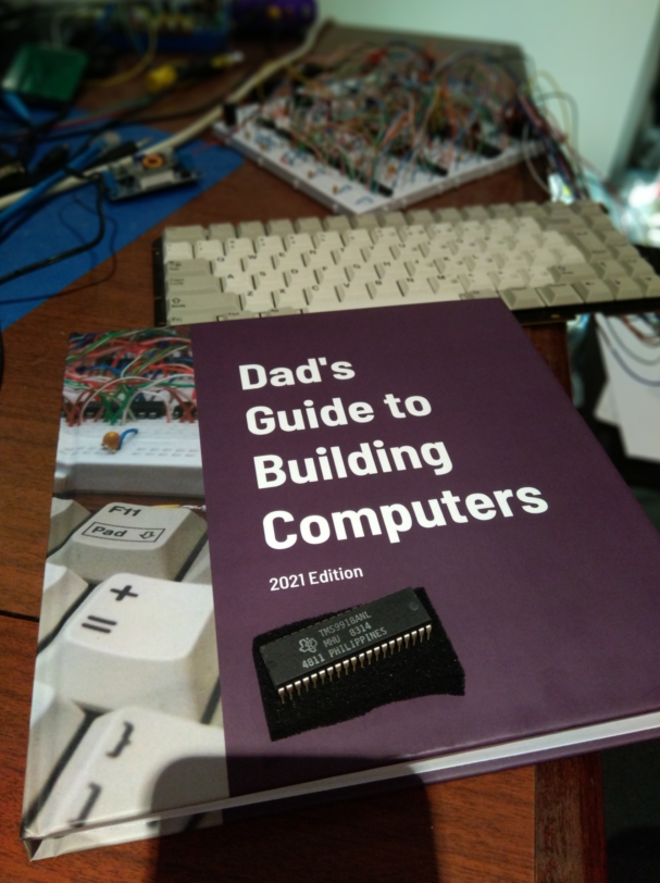
Anyway, after I finished the breadboard Colecovision I thought a full MSX computer might be achievable. It uses the same video chip and CPU as the Coleco, but this time its a full computer with a keyboard. It has a few more chips than the Coleco, but I always have ideas about what can be thrown out to keep the size down. I came up with a schematic … and then promptly postponed making it for a few years. But I’m a big one for ‘summer projects’ , and this past summer I had a big motivation to ‘write a book on how to construct a computer on a breadboard’ for my son to read and I thought the MSX computer would be a good one to write about. So here it is:
Well, it’s the computer, not the book obviously. The book is actually proving harder to make than the computer . The computer seems to run a lot of stuff. It doesn’t run every piece of MSX software but seems to run quite a lot. I’ve just got it loading some simple ROMs (16 and 32K types) and also loading stuff from cassette.
 |
 |
 |
 |
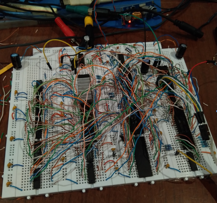
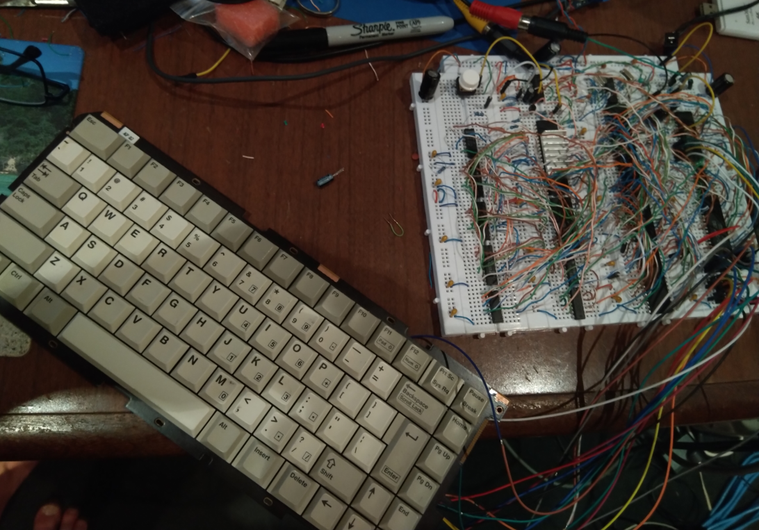
Whereas the Coleco and Funvision could fit in three 840 point breadboards, the MSX computer ‘just’ squeezes into four of them. OK, so the keyboard is not on a breadboard. I had to compromise somewhere. But you can potentially leave it off and still use the computer as a console with a joystick.
Apologies for the brevity of this post. I wanted to do a long article with lots of detailed construction photos but it just ended up way too long. The book ended up at 240 pages and it was too hard to condense down.
The recipe
OK, so what makes up an MSX computer?
- Z80A CPU running at 3.579545MHz
- TMS9918A or TMS9928A or TMS9929A video chip depending on what country you were in in the 80s. There’s 16Kbytes of dynamic RAM attached to the video chip. I know lots about these video chips. They are pretty cool and easy to interface to and the general public could buy them in the 1980s.
- Some RAM for the CPU. Generally this was 64KBytes of dynamic RAM , most likely as eight 4164s
- AY-3-8910 sound chip.
- 8255 peripheral chip.
- A boot ROM most likely 32Kbytes in size containing a BASIC interpreter.
- Some 74LS logic gluing it all together
- One or more cartridge slots
They had a full QWERTY keyboard (or AZERTY or whatever) and two joystick ports. They had a built in cassette port and there were options to add disk drives etc. They have a simple bank switching memory scheme where you can have four ‘slots’ of 64KBytes; slot 0, slot 1, slot 2 and slot 3. So you could potentially have ‘up to 256KBytes’. The boot/BASIC ROM sits in slot 0, the cartridge slots are generally slot 1 and 2 and often slot 3 is 64KBytes of RAM. The bank switching scheme used one port of the 8255 and a 74LS153 to let you swap 16KB chunks of the memory space in and out of the 64KB that was visible to the Z80A. For example, you could have 0x0000 to 0x3fff as being from the ROM in slot 0, and 0x8000 to 0xbfff from the RAM in slot 3.
If you were in Australia or New Zealand or other PAL country then your MSX computer would have had a TMS9929A video chip and circuitry to convert its Y, B-Y, R-Y outputs to composite PAL video. If you were in the USA or Japan or other NTSC country then you probably had a TMS9928A again with circuitry to convert the Y, B-Y and R-Y to composite NTSC or a TMS9918A (actually I am not sure if any had the 9918). The TMS9918A has built in circuitry such that it can produce an NTSC colour composite signal (so long as you add a transistor and a couple of resistors)
So the video chip needs a 10.738635MHz cystal. The sound chip uses a 1.789772MHz clock , which is just the 3.579545MHz CPU clock divided by two.
My recipe
So this MSX computer is a bit different to MSX computers from back in the day. Here’s a list of what I changed. A key motivator was to ‘squeeze it into the least number of 840 point breadboards possible’.
- Instead of a 10.738635MHz crystal I use a 21.47727MHz crystal which I think is easier to obtain. Using a technology called ‘dividing by 2’ I just divide 21.47727 by 2 to get 10.738635MHz for the video chip
- I used a TMS9918A. When I was a kid (in Australia) the TMS9918A was a completely pointless chip since it produced an NTSC colour composite signal and there were no NTSC TVs in Australia in the 1980s. But, in 2021 if you still have a TV that has a composite input there is a fair chance it will accept an NTSC colour composite signal regardless of what country you are in. If you’ve got a monitor that accepts composite, again there’s a fair chance it accepts NTSC colour composite. And if you don’t then there are adapters/converters that will convert NTSC composite into VGA or HDMI or some such. I recently bought a retrotink mini … which is rather awesome even if it is a bit pricey. Otherwise I use a Dell 2001FP monitor (I have pre June 2005 ones, but I think for composite the later ones work fine). I also have several cheap composite to VGA converters from ebay and none of them work, so don’t get one of those. Perhaps the main reason for using the TMS9918A is I don’t have to mess with trying to convert Y, B-Y and R-Y to composite or component video (you can spend hours or days on the internet researching this ‘component’ story for these chips).
- The TMS9918A would normally have eight 4116 DRAMs attached if this was the 1980s. They annoyingly need multiple power supplies and in 2021 they are also quite hard to find. I had toyed with using eight 4164s like I did with the Funvision and Colecovision projects, but even 4164s are hard to get these days. Instead I’m going to use a 32K static RAM and quite a bit of extra circuitry to make it work with the TMS9918A. It’s a reasonably straight forward idea using latches and some inverters to make it work, and I certainly won’t take credit for the idea as several other projects on the net use this same idea.
- Instead of dynamic RAM for the CPU I just have one big 128KB static RAM which will occupy slots 2 and 3 (in hindsight it is probably a waste having it available in slot 2).
- I used an AY-3-8912 sound chip instead of an AY-3-8910. The 8912 has the same sound chip stuff inside it, but instead of two general purpose 8 bit IO ports like the 8910, the 8912 only has one 8 bit port. The net result is that instead of a 40 pin chip, the 8912 is a 28 pin one. That just means I get back a little more breadboard space. Technically you can squeeze an AY-3-8910 in instead, but you ‘ll struggle to fit in the cassette interface circuitry (which is fine if you are never going to load cassette based programs). What do you lose out on by using the AY-3-8912? Well, it makes it impossible to have two joysticks. The way the joystick interface works on a normal MSX computer is that the two joysticks are multiplexed into some pins of port A of the AY-3-8910, but it uses an IO pin on port B to indicate which joystick is being read (ie. an IO pin of the 2nd IO port). The net result is that most games that are single player will work fine, but ones having a two player mode will be totally confused by both players appearing to move their joysticks in unison.
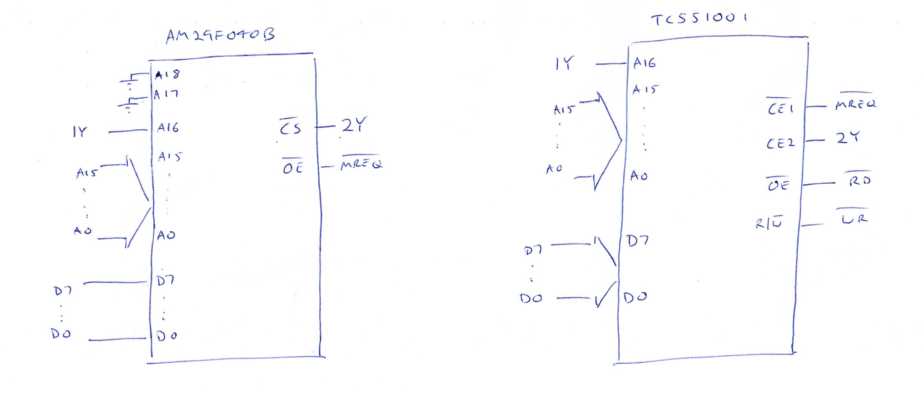
- Instead of a 32KB boot ROM, I’m using a 512KB flash ROM. It will appear as 128KB of memory across slot 0 and 1 though. You can then make the 32KB boot ROM still appear in slot 0 by writing it to the first 64KB of that 128KB, and you can optionally write a cartridge image into the second 64KB since it will appear as slot 1. Because 128KB is a quarter of the ROM, you can effectively put four different things on the ROM and flip between them by changing the two highest address lines of the flash ROM.
- There is still a fair bit of 74LS logic (I used 74LS since I seem to have a stockpile but modern 74HCT or 74ABT should work too), but I am leaving out various buffers and tranceivers used for the cartridge port (since there isn’t a cartridge port), and there are a few other spots like IO access for the sound chip where I’ve put in the ‘bare minimum’ to make it all go.
Layout and Chips
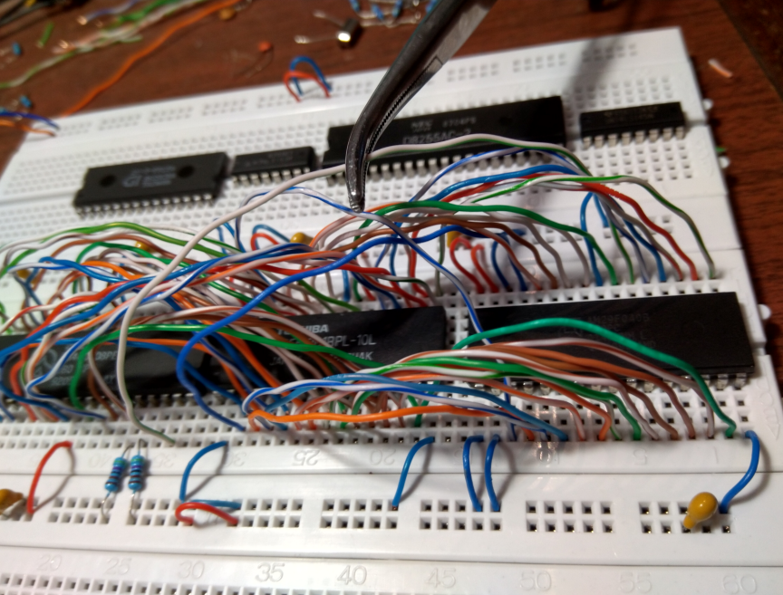
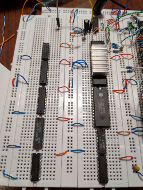
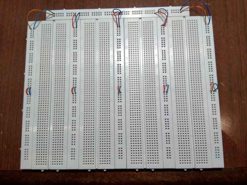 So it’s basically four 840 point breadboards hooked together. They are arranged so that there is one ‘power strip’ between each of the main sections and another power strip across the top. I used Multicomp brand breadboards that I bought from element14. I have an article elsewhere on my blog highlighting the problems with using the really cheap breadboards you find on ebay/aliexpress. Don’t use them. It’s not worth the pain. Search element14/mouser/rs-online/digikey etc for breadboards and buy them from there.
I’ve got some small orange and blue wires shown. These are for the +5V and GND rails. I would have used red and black except I used solid core ethernet wires for the entire project.
Here’s the placement of chips. Ignore the crystal clock wiring that’s already there. I just forgot to take a photo prior to this.
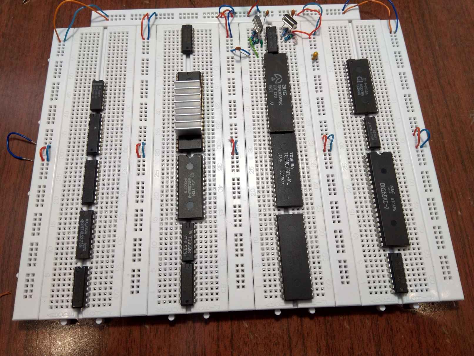
The table below shows the four columns of chips and how I placed them.
| Leave 5 rows | the 1st 74LS74 | leave 1 row | leave 11 rows |
| the 2nd 74LS74 (not shown) |
leave 6 rows | 74HCU04 | AY-3-8912 |
| leave 3 rows | TMS9918A | leave 1 row | leave 1 row |
| 74HC14 | leave 1 row | Z80A | 74LS153 |
| leave 1 row | 62256 | leave 1 row | leave 1 row |
| 1st 74LS374 | leave 1 row | TC551001 | 8255 |
| leave 1 row | 74LS32 | leave 2 rows | leave 1 row |
| 2nd 74LS374 | leave 1 row | AM29F040B | 74LS145 |
| leave 1 row | 74LS00 | ||
| 74LS373 | |||
| leave 1 row | |||
| 74LS138 |
Per the table , you’ll note I ended up putting a 2nd 74LS74 in the top left. I originally left out the compulsory WAIT state circuitry that all MSX computers have for M1 cycles thinking ‘surely this would still work without it’. Suffice to say that lots of games do not work properly without the compulsory WAIT states. I’ll try to remember to add some more detail later in this blog post. It was an interesting issue.
In theory you should be able to swap the 74LS parts for 74HCT or 74ABT, but I haven’t tried. As for the other parts
- Z80A. You can actually buy these brand new in 2021. Well, you can buy faster parts brand new in 2021. The Z80A was ‘maximum 4MHz clock’. When I checked mouser recently (2021) you can get 6MHz or 8MHz or 10MHz or 20MHz versions. Any of these will do. You obviously want a DIP version. I’ll note that I bought about 10 ‘cheap’ 20MHz Z80’s on ebay a few years ago and most of them did not work in the MSX computer when I tried. Awesome … not. Beware fakes.
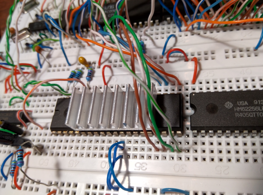
- TMS9918A (or often TMS9918ANL). You’ll need to go on ebay or aliexpress to get these. I’ve actually bought quite a few of these on ebay/aliexpress and they all work OK. You need a heatsink of some sort. You’ll see I’ve got a reasonable size rectangular one. I can’t remember where I got it. Worst case you could put one of those little raspberry pi heatsinks on it, but I would not recommend it. Again, I think there are fakes of these chips out there too these days, though I have bought heaps of cheap 9929’s, 9918’s and 9928 and they all seem to work ok.
- AY-3-8912. Again, find these on ebay/aliexpress. Technically you should get the AY-3-8912, not the AY-3-8912A since the latter is missing internal pullup resistors but I’ve actually tried both and they both seemed to work OK.
- 74HCU04. Yep, it has a ‘U’ in the middle. These make great crystal oscillators. Technically a 74HC04 (without the ‘U’) should work, but I bought a heap of 74HC04’s from some ebay/aliepress seller and none of them worked as crystal oscillators. They worked as simple inverters. Just not as crystal oscillators. The one’s from my local Jaycar work fine. What the. The 74HCU04’s are harder to get on ebay/aliexpress, so I’m hoping if you bothered to build this you would just give up and order them from a proper electronics distributor (insert mouser/rs-online/element14 etc) and then the crystal oscillators should just work because you won’t have a fake one.
- TC551001. I got a bunch of these off ebay/aliexpress. There’s actually a new equivalent, the AS6C1008 that should work too, but I have not tried it.
- AM29F040B. I just got some of these on ebay/aliexpress. The one’s I have are obvious fakes, but work fine. An alternative is the SST39SF040. It is also a DIP 512KB flash ROM and is available new at a lot of distributors. I used the AM29F040B as I built an Arduino based programmer for them a while back, and more recently I’ve made an STM32 based flash ROM programmer as well for the AM29F040B.
- 8255. Either ebay/aliexpress or I think the 82C55 is available new.
- 74LS145. I’ll mention this one as I don’t think there is a 74HCT version. So you’ll need to hunt ebay/aliexpress for it. You can in theory use a 74LS138 and an inverter instead. I will leave that up to the reader.
Clocks
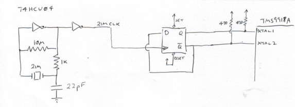
We’re going to use the 74HCU04 to make two crystal oscillators. An MSX computer actually needs three main clock frequencies
- 3.579545MHz for the CPU clock
- 1.789772MHz for the AY-3-8912 PSG (sound chip) clock
- 10.738635MHz for the TMS9918A
I originally thought it was near impossible to get 10.738635MHz crystals in 2021 and so discovered that 21.47727MHz crystals were more plentiful and so decided that this computer should have a a 21.47727MHz oscillator that is then divided by 2 to get 10.738635MHz. I have since discovered that the likes of Mouser do sell the 10.738635MHz crystals. But anyway.
So the 3.579454Mhz clock looks like this with one half a 74LS74 doing the divide by 2 to get the 1.789772Mhz PSG clock
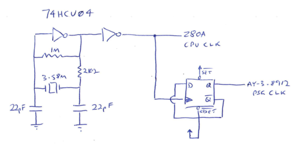
And the 10.738635MHz clock is like so. First a crystal oscillator for a 21.47727MHz crystal which we divide by 2 before driving the VDP chip.
The Z80A, RAM chip and ROM chip
My short term goal with any computer is to ‘first put enough chips and wiring in to get it to blink an LED’. Once I confirm I can blink an LED then I continue on and do the rest of it. Basically we’ll do this first.
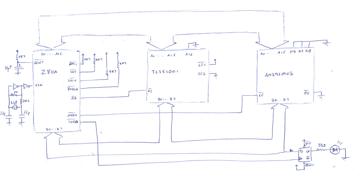
Yep, the TC551001 static RAM chip is effectively disabled (connecting its _OE to Z80 _RD is just a reminder to myself that later on this fixes an edge case). Disabling the TC551001 was deliberate as it physically sits between the Z80A and the AM29F040B (which is at the bottom of the breadboard to make it easier to remove). The entire lowest 64K of the flash ROM takes up the entire Z80 address space and any write to an IO address will latch D0 into the D flip flop and allow us to turn the LED on and off.
Here’s the blink program I used
0000                            ORG     $0000000

0000  3E 01                     ld a,$01
0002  D3 80             top     out ($80),a
0004  47                        ld b,a

0005  11 FFFF                   ld de,$ffff
0008  1B                loop1   dec de
0009  7A                        ld a,d
000A  B3                        or e
000B  20 FB                     jr nz,loop1

000D  78                        ld a,b
000E  3C                        inc a
000F  18 F1                     jr top
I just used asmx to assemble it. It’s simple enough that you can hand assemble it (ie. look up opcodes in books. I did this a lot when i was a kid). If you can’t be bothered assembling, you can actually generate the binary in a one liner perl program
echo -en "\x3e\x01\xd3\x80\x47\x11\xff\xff\x1b\x7a\xb3\x20\xfb\x78\x3c\x18\xf1" >blink.bin
I updated the arduino flash ROM programmer project I have so that it works with a stm32f407 board. There are notes at https://github.com/kernelcrash/stm32-flash-rom-programmer. You can use it to program the blink.bin.
You can see in some of the photos I put 100nF decoupling caps all over the place, and also a few larger electrolytics towards the top of each supply rail.
Power on, and if everything is wired correctly you should get a blinking LED. If you don’t, go back check wiring, check you programmed the flash ROM correctly and don’t read any further until you have the LED flashing.
The Video Display Processor (VDP) circuitry
So LED blinking is sorted. Now we can move on.
So the TMS9918A/9928A/9929A chips have been around for a long time. They had a heap of built in circuitry that simplified connecting them to eight 4Kbit or 16KBit Dynamic RAM chips. most designs had eight 16Kbit DRAMs like the 4116 chips. Being 16Kbit it needs 14 address pins, but these are multiplexed together on 7 address pins. ie. in a memory cycle an external system provides the first of the 7 address bits and sends _RAS low, then it applies the 2nd 7 address bits and sends _CAS low. We need to do the opposite since we’re using a static RAM chip that can potentially take all 14 address pins at the same time. I’m using a 32Kbyte 62256 Static RAM chip. These are common and cheap. Being 32KB it has 15 address lines, so we’ll tie the highest address pin A14 to GND effectively making it a 16KB RAM. We’ll demultiplex the addresses by using a series of latches. When _RAS goes low we latch the first 7 address bits. When _CAS goes low we latch the 2nd 7 address bits. Now we have our 14 address bits. We also need another latch for the data bus as the VDP put data out the address lines during a write cycle
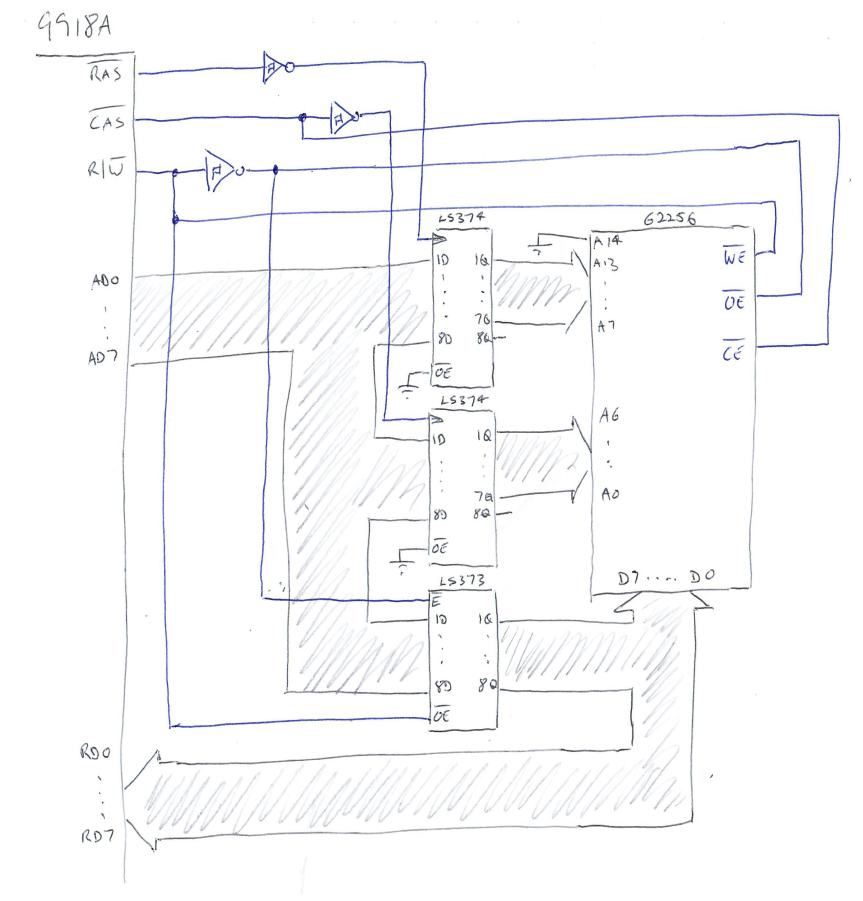
I’m using some schmitt trigger inverters out of a 74HC14 when driving the CLK and E pins of the latches. For starters _RAS and _CAS have a negative going edge, whereas the latches effectively have a positive going edge, so we need to invert the signals. There’s a problem too with _RAS and _CAS in that they sort of go low slightly too early. I think the VDP chips factored in just how slow the 4116’s were at latching the address so sent it slightly earlier than you would normally do. In our case the schmitt triggers add a bit more delay than what you would get with a normal inverter like a 74LS04.
Next wire up power to the Video circuitry chips. Most of the orange and blue wires are straight forward and connect as per the pinouts for the requisite chips. However, note the three blue wires connected to the GND pin of the VDP chip. This is deliberate. It is a power hungry chip, and I will be honest in saying that breadboards aren’t exactly designed for delivering lots of power.
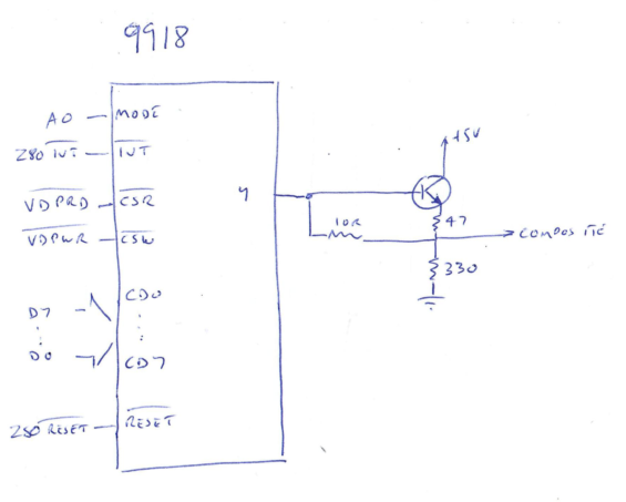
Connect the data lines between the Z80A and the 9918A. Now, if you’re referring to the TI datasheet for the 9918A you’ll note that these are the pins CD0 to CD7. Due to some anomaly of history, TI decided that CD0 was the most significant bit, and CD7 the least significant. This just means you sort of have to wire it backwards. So the Z80A D0 goes to the 9918A CD7 (brown wire), Z80A D1 goes to 9918A CD6 (white-brown) and do on through to the Z80A D7 going to the 9918A CD0 (white-blue). The same sort of reversed naming occurs for the AD0 to AD7 pins (AD0 is the most significant one) and RD0 to RD7 (again RD0 is the most significant one).
Here’s a shot with the latches wired up to both the VDP and 62256 static RAM
IO decoding
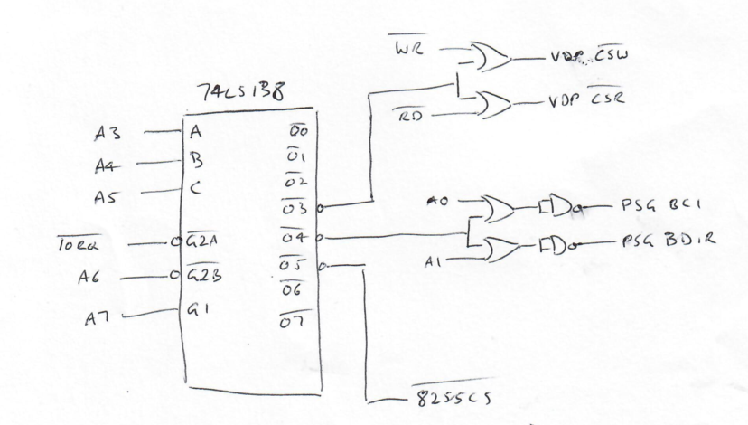
To read/write to the VDP and the other IO chips we need a 74LS138 and a few gates doing some address mapping. We only really need 3 IO devices mapped in order for the computer to be like an MSX computer. IO address 0x98 to 0x9f is the VDP chip. IO address 0xa0 to 0xa7 is the AY-3-8912 and 0xa8 to 0xaf is the 8255 peripheral chip.
Here’s some other pins of the VDP chip to wire up including the composite video output circuirtry. I just used a BC547 for the NPN transistor.
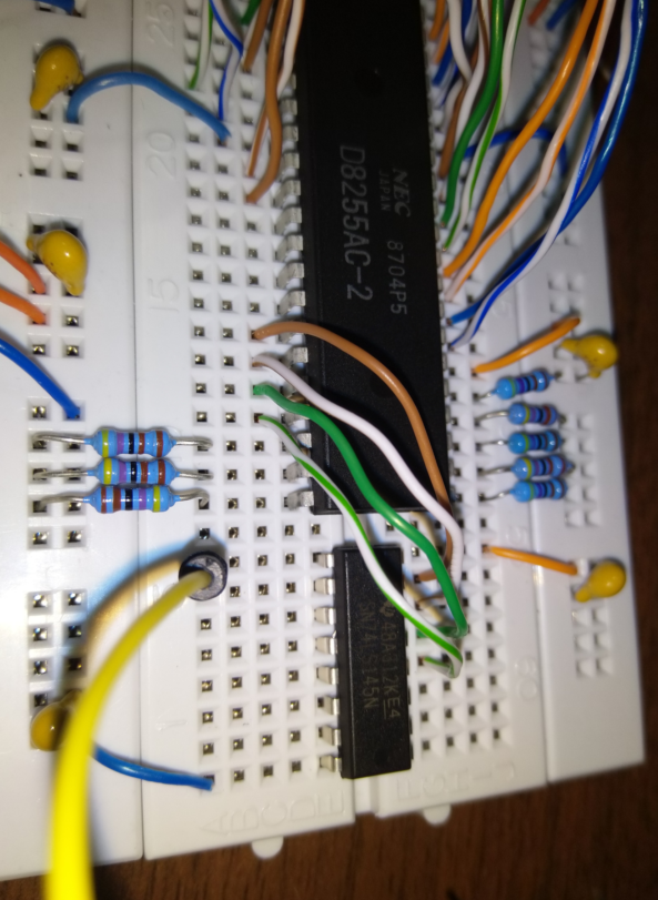
And the 8255 and AY-3-8912. Port B of the 8255 and the 74LS145 will connect to a keyboard matrix. You can actually start a lot of games just by working out the pins of the 74LS145 and Port B to short together in order to press 1 , 2 and space.
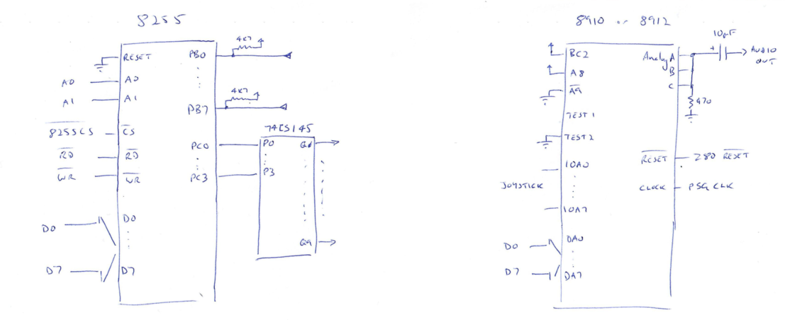
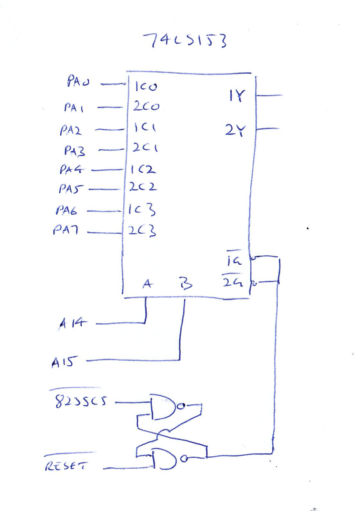
Port A of the 8255 is used for MSX’s bank switching. We need a couple of 74LS00 NAND gates as a simple flip flop such that after reset, the 1Y and 2Y outputs of the 74LS153 are both zero. This means the computer will always boot up on bank 0 of the four banks.
Memory
Now we need to rewire the TC551001 128K static RAM and the AM29F040B 512K flash ROM. The lowest 128K of the flash ROM appears as all of slots 0 and 1. And the 128K of the static RAM appears as all of slots 2 and 3 (in hindsight this is a bit of a waste, but because of the two chip selects on the static RAM it is somewhat easier). You’ll see that the 1Y and 2Y outputs of the 74LS153 go to various pins of the static RAM and flash ROM to make them appear in the appropriate ‘slots’.
So in a normal MSX computer it will boot from the ROM at the bottom of slot 0. In our case the first 64K of the flash ROM is taking up all of slot 0. I think most if not all MSX (v1) ROMS were the 32K BASIC ROM. In my case I used the one from the V-20 flashed into the bottom 32K. If you just did that it should boot to BASIC only. If you wanted to boot to a simple cartridge ROM (eg. an older 16K or 32K cart) then you would still flash the 32K BASIC ROM to 0x00000, but then also flash the cartridge dump to 0x14000 of the flash ROM (ie. 0x4000 in slot 1). I’ll note here that there is no fancy ‘Mapper’ support so you are limited to these simple 16 and 32K ROMs (though I was able to mod some of the Coleco conversions so that they worked without Mapper logic).
Now the flash ROM is a 512KB one, yet so far only the first 128KB of it is used for slots 0 and 1. What we can do is to write different things to the three other 128KB chunks of the flash ROM, then tie the A17 and A18 pins to +5V and GND as appropriate to select these other 128KB chunks. As an example, if you want to also have the cartridge game Pippols available on the flash ROM, you would write the 32KB BASIC ROM to address 0x20000 , and the cartridge itself to 0x34000. Then you’d tie A17 to +5V and A18 still on GND. Power on and it should run Pippols. Similarly, to use the 3rd chunk you’d write BASIC to 0x40000, and the cart to 0x54000 and power on with A17 low and A18 high. And for the fourth chunk BASIC at 0x60000 and the cart at 0x74000 and power on with both A17 and A18 high.
WAIT states
All MSX computers have a circuit like this that inserts a single WAIT state during a Z80A M1 cycle. If you have no idea what this means, it slows down some but not all of the memory accesses that the Z80A does.
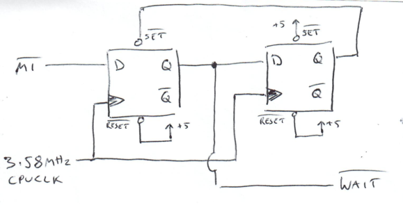
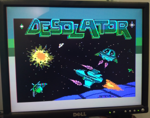
I originally left this circuit entirely off and a lot of games seemed to work, but some were just a bit weird having graphical errors on screen. A good test one I found is Desolator. It just had weird graphical errors until I put the WAIT circuitry in. The reason I left the circuitry off is I pigheadedly thought ‘I am using a fast Flash ROM and fast Static RAM. There is no need for WAIT states’. What I forgot is that the rate at which you can read and write data to/from the VDP chip is actually quite slow. Let me rephrase that. The VDP won’t work properly if you read or write to it too quickly. As a lot of games would have been trying to read or write to the VDP at the fastest rate that would work, they might have had NOPs and other things to get that throughput at the exact fastest rate for a 3.579545MHz Z80A with WAIT states on M1 cycles. As I originally had no WAIT states, the Z80A would have been reading/writing marginally faster … and marginally faster is enough to screw things up.
Anyway, that’s what the extra 74LS74 is for in the top left corner.
Keyboard and Joystick
Wire up a DB9 male socket like so
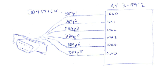
Hopefully it looks something like this. You just need to get an Atari style joystick to plug in to it. I’ve also used a cheap Genesis MegaDrive controller, but you need to do some slightly different wiring (DB9 p5 goes to +5V, DB9 p7 goes to +5V. The rest are the same)
For the keyboard, you can initially leave it off if you just want to try some cartridge ROMs. Most carts seem to want you to press 1, 2 or SPACE, so you can just have a little jumper wire (like the yellow one below). In the photo one end of the jumper is connected to pin 1 of the 74LS145 (Q0). the other end is floating free below the breadboard. To pretend you are pressing ‘1’ on the MSX keyboard you tap the floating end of the wire to p19 of the 8255. To press ‘2’ you tap the floating end to p20 of the 8255. In order press space you need to pull out the yellow jumper entirely. Plug one end to p10 (Q8) of the 74LS145. Then tap the free end to p18 of the 8255.
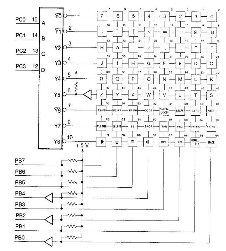
You can do a real keyboard too. The Canon V-20 service manual has this handy diagram of the key matrix. You just need to wire up a keyboard exactly like this.
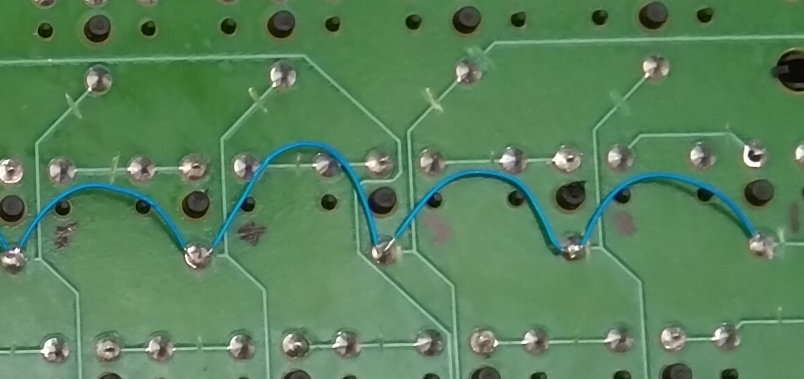
I have an old Cherry keyboard. It’s been butchered in the past so that it can be rewired to any key matrix I so choose. That just means cutting lots of traces on the keyboards actual circuit traces, then replacing it with little wires connecting it how you want it. Here’s an example of some of the cuts and the beginnings of the wiring. It’s hard to see but this is the number row of keys (5, 4, 3, 2 and 1)
And lots of wires
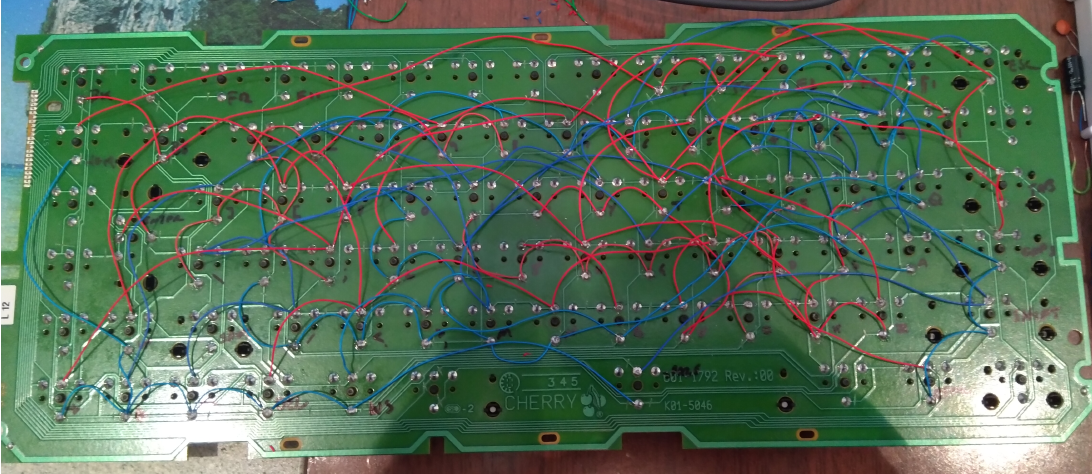
And here it is all hooked up.
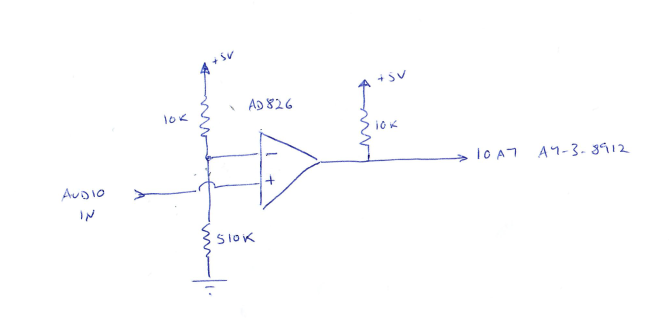
Cassette Input
In order to load programs from cassette (or most likely a modern computer playing WAV files of cassette dumps), I built the following with a little AD826 opamp I had handy. There’s enough space above the AY-3-8912 for this circuit
Getting it going
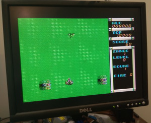
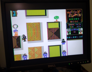
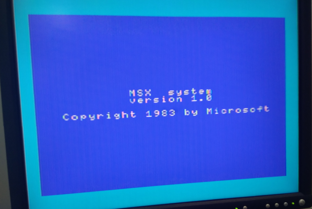
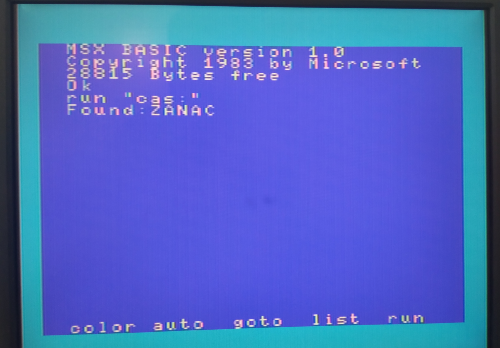
When you power on you should get a startup screen like so;
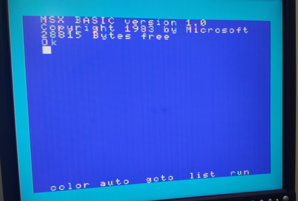
And a second or two later this screen (28815 bytes free is correct)
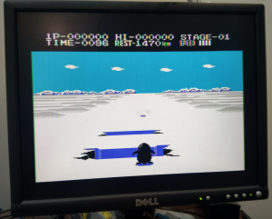
If you have a small jumper hooked up for pressing ‘1’ or ‘2’, try that and see if a 1 or 2 appears on the screen. I would probably power down at this stage, and write the BASIC ROM at 0x20000, and a simple cart like Antarctic Adventure to 0x34000, then change A17 of the flash ROM so its connected to +5V. Power up again and see if Antarctic Adventure starts up. Press ‘1’ I think for joystick mode and assuming you have a joystick try playing the game.
Loading stuff into the cassette interface
Generally you need a modern computer with its audio output connected to the cassette input circuitry (probably just LEFT or RIGHT audio should be fine). Turn the volume up high initially. You either get WAV file dumps of some MSX v1 games, or CAS file dumps and then use a tool to convert them to WAV files (I just used the cas2wav tool at https://github.com/rcmolina/castools). So you could enter
castools/cas2wav somegame.cas somegame.wav
I usually use mplayer (on linux) to play it out the audio. Most MSX cassette dumps will have in the filename letters like “[RUN\’CAS-\’\]” or “[BLOAD\’CAS-\’\]”. This is actually an indication of what to type on the MSX comuter to load the file. As an example, if I wanted to load ZANAC and the filename has [RUN\’CAS-\’\] in it , I would enter this first on the MSX computer and hit ENTER
run "cas:"
Now run mplayer on your modern computer. Hopefully within about 10 seconds you will see something like
If you don’t see that , power off, check wiring, try again. Because this is ‘loading from cassette’ it can be quite slow, so if the game does not load in 3 or 4 minutes (you can see whether mplayer is still playing or not), then try lowering the volume of the modern computer and trying again. This is probably obvious, but if you are playing any other sounds on your modern computer then that will interfere with the cassette loading on the MSX computer. I actually tested this a lot with a raspberry pi. You can have the rPi playing the cassette noises while you do something else on your modern computer.
Anyway, it should eventually load
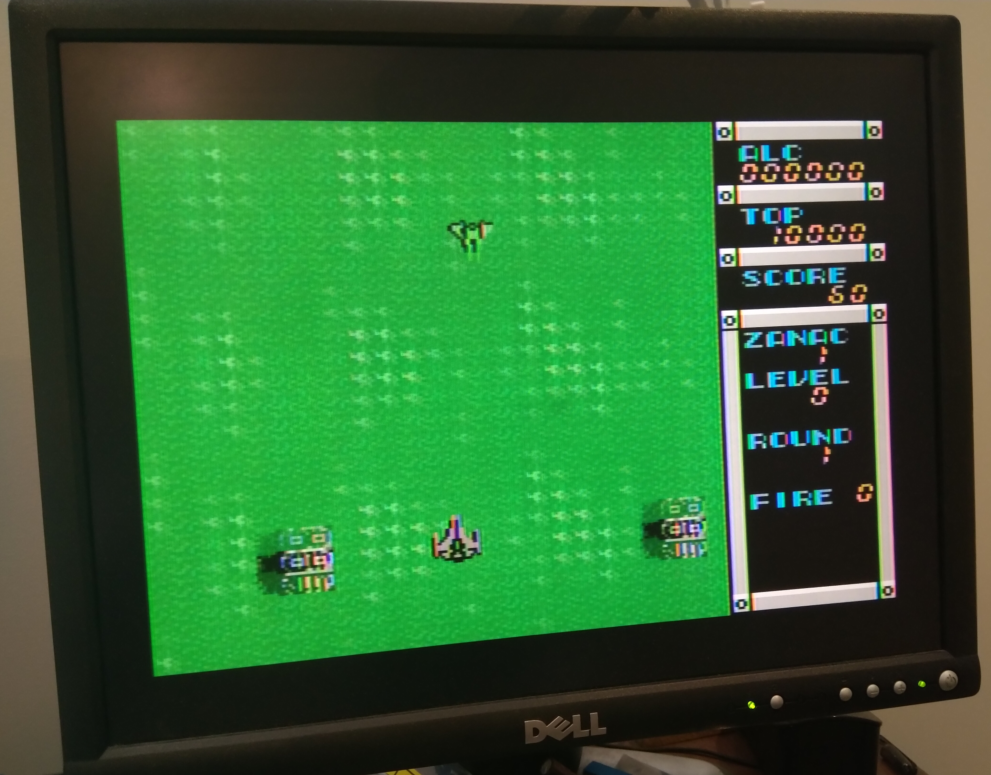
That is pretty much it.
I did eventually finish writing the book, and my son was able to construct it from the book, so now I can move on to something else.